Bluetooth Antenna — Tools & Topics
Best Bluetooth Antenna project topics for BE, BTech and MTech students. Full-wave EM simulation with HFSS, CST, COMSOL and FEKO plus fabrication and measurement guidance.
Packages include simulation notes, S-parameter/pattern interpretation, university-format report, PPT and viva Q&A.
Tools & Platforms
Project Overview & Technical Details
Abstract, simulation tools, fabrication dimensions and expected metrics for Bluetooth Antenna.
Abstract
The Bluetooth Antenna project focuses on the electromagnetic design and performance analysis of an antenna structure intended for its target wireless application. The study considers the antenna geometry, substrate or dielectric environment, conducting elements, excitation method, and surrounding boundaries so that the proposed configuration can be evaluated under realistic operating conditions.
The design process begins with suitable antenna dimensions and material parameters derived from the intended operating requirements. The selected operating region of 2.4 GHz is considered during the initial design and tuning. Key geometric parameters can be varied to study their influence on impedance matching, bandwidth, radiation behaviour, efficiency, and gain.
Full-wave electromagnetic simulation is used to examine the behaviour of the proposed Bluetooth Antenna before fabrication. Ansys HFSS and CST Studio Suite are suitable for this type of antenna investigation because they support detailed electromagnetic field analysis and extraction of parameters such as S-parameters, resonant response, radiation patterns, gain, directivity, and field distributions.
During optimization, parameters such as feed position, element dimensions, spacing, substrate properties, and other project-specific geometric features can be adjusted to obtain the required response. Simulation results can be compared across design iterations to identify a practical configuration while reducing unnecessary fabrication trials and helping validate the expected antenna characteristics.
The completed study provides a structured basis for antenna fabrication and experimental verification. The simulated results can be used to prepare performance plots and design documentation, followed by measurements such as return loss, impedance response, radiation pattern, gain, or other application-specific characteristics. This approach supports systematic evaluation of the Bluetooth Antenna for academic research, prototype development, and wireless communication applications.
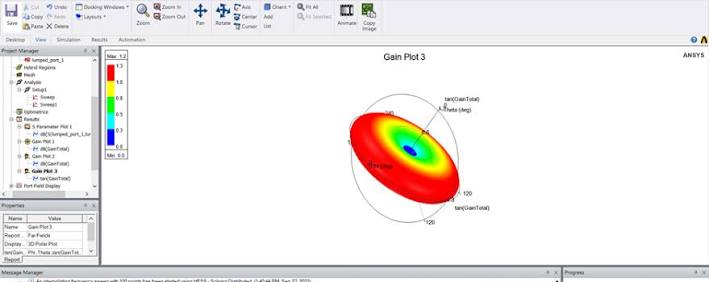
Simulation Tools Used
HFSS / CST with enclosure model; VNA matching
Typical workflow: geometry → boundary conditions → parametric sweep → S-parameter & far-field post-processing → optimization.
Operating Frequency
2.402–2.480 GHz
Antenna Dimensions (Typical)
Chip antenna footprint few mm; or PCB inverted-F ≈ 25 × 5 mm
Feed Network
50 Ω microstrip to module pin; pi-matching network
Fabrication Details
FR-4 module PCB; chip antenna or printed IFA
Key Performance Metrics
S11 in free space vs installed; range tests
Deliverables for Students
Simulation project files (HFSS/CST), dimensioned drawings, S11 / Smith / pattern plots, comparison table (sim vs target), university-format report, PPT and viva Q&A support from Bangalore.
Contact us for full simulation setup, fabrication guidance, university-format report, PPT and viva Q&A.
Why Choose Us?
Bangalore guidance for RF and antenna engineering students.
EM Simulation
HFSS, CST, COMSOL and FEKO workflows with mesh, S-parameters and pattern analysis.
Design Metrics
Return loss, gain, efficiency, axial ratio and mutual coupling interpretation.
Fabrication
PCB guidelines, VNA measurement concepts and sim-vs-measured comparison.
Report & Viva
University-format documentation, PPT and expected viva questions.
FAQ
Antenna / RF Lab — Bangalore
Simulation and measurement support for antenna projects.
Full-Wave
Studio
RF Module
MoM
& Gain
& VNA
& MIMO