Chapter 7
© 2012 Fagerstrom and Bengiamin, licensee InTech. This is an open access chapter distributed under the terms of the Creative Commons Attribution License (http://creativecommons.org/licenses/by/3.0), which permits unrestricted use, distribution, and reproduction in any medium, provided the original work is properly cited.
Sven Fagerstrom And Nagy Bengiamin
Additional information is available at the end of the chapter
1. Introduction
Advances in semiconductor technologies to produce high power devices have facilitated numerous applications where high power density is a key for practical and sophisticated solutions. Instead of being limited to the traditional low power electronics applications, high power devices opened a broad frontier for engineering design. These devices are now embedded in systems that span the full range from small electric motor drives to very high voltage transmission lines where hundreds of amperes are regulated while the devices are exposed to thousands of volts. Compared to the traditional rotating electric machine based (dynamic) energy conversion, these devices made static conversion from one form of electricity to another so seamless that employing a certain form of electric power (AC, DC, or a combination) has become an engineering design option rather than a forced solution.
Application areas like in motor drives, fuel cells, solar panels, wind turbines, electric cars, and high speed transportation systems are only a few of the major beneficiaries of advances in power electronics. Emphases on energy conservation motivated the design for improved system efficiency where power electronics devices are utilized in their most desirable mode.
These efforts resulted in increased portability of high power density systems and affected the design of the full range of power systems including those for small electronic equipment which are becoming more demanding on power for their ever increasing features and capabilities. Like all advanced engineering design applications, mathematical developments and supporting software tools for modeling, simulation and analysis are critical (Shaffer, 2007; Assi, 2011). In addition to introducing some of the fundamental concepts in power electronics and related applications, this chapter exploits the capabilities of Matlab and its associated SimPower and Simulink toolboxes as an effective relevant engineering tool.
When dealing with an alternating current, changing voltage levels, at the same frequency, is achieved simply by utilizing AC transformers where the principle of mutual induction MATLAB – A Fundamental Tool for Scientific Computing and Engineering Applications – Volume 1
134
exists between two magnetic coils with the proper turns-ratio. Mutual induction is possible due to the rate at which the magnetic lines cut the wires of the transformer coils and the produced electromotive force that is capable of producing current in closed electric loops.
This fundamental concept is not applicable to DC voltage and current due to the absence of the alternating nature of the produced magnetic fields. Therefore, changing DC voltage from one level to another must be achieved using different methodologies. One possible methodology is to modulate DC voltages by switching them on and off at proper rates and durations such that the average produced voltage is controlled. The key concept here is to store energy then release it at the proper time with the proper rate needed for the desired load. Energy storage elements like inductors and capacitors facilitate this methodology.
Therefore, a combination of energy storage elements and switching schemes provide the basic ingredients for the design of DC-DC conversion devices. Such devices are referred to as power electronic DC-DC converters. The modes of operation of these devices are dependent on the shape of the produced voltage waveform which is manipulated by the switching scheme and the size of the energy storage elements. Compared to AC transformers which usually exhibit linear characteristics for its most modes of operation, DC transformers (DC-DC converters) possess highly non-linear characteristics which require more intensive analysis and design schemes.
Optimization of power electronics systems’ design and operation is important to accommodate the growing need for energy efficiency in portable electronic devices to extend their battery life and respond to their increasing functionality and features. These features demand more electric power while the devices must reduce in size and weight; i.e.
increased energy density. DC-DC converters are embedded in numerous electronic equipment and they have become an integral part of many commercial and industrial products. These converters are employed to lower (buck) or raise (boost) DC voltage levels as needed by the application. Buck and boost converters are emphasized in this chapter for their different topologies and modes of operation. The presented methodologies facilitate analysis, characterization, and design of efficient DC-DC converters. Sufficient background and theoretical development are provided for completeness.
2. Static Power Converters
Static power converters can take numerous topologies which enable AC-AC, AC-DC, DC- AC, and DC-DC conversion. AC-AC converters vary in complexity from the crude chopping of the AC waveform in order to regulate the delivered average power like in light dimmers and electric stove burners to varying the produced frequency like in Variable Speed Drives (VSD) for AC motors. AC-DC converters usually utilize the simple rectifier bridge configuration. They are popular in windmill applications as a front stage before converting to AC for interface with the utility grid. This last stage employs the DC-AC converter which is also popular in applications like solar panels interface with the utility grid. In addition to the AC-DC converter, most household and commercial electronic equipment use DC-DC Modelling and Characterization of Power Electronics Converters Using Matlab Tools 135 converters. These converters produce the multiple DC voltage levels necessary for the operation of the equipment. DC-DC converters are also critical for battery powered portable electronic devices where power density is high and efficiency of converters is critical to the charging cycle of the device.
2.1. Ac-Ac Converter
Converting AC at the same frequency is most effectively achieved using induction transformers. This is particularly true for high frequency/low-power applications where the magnetic core is relatively small. Applications that require converting to different frequencies, however, can be achieved in several configurations. One configuration may utilize an intermediate stage of AC-DC back-to-back with DC-AC as is the case for wind energy conversion for example; assuming that the wind turbine is coupled to an AC electric generator. Cycloconverters (Rashid, 2004) on the other hand, don’t require an intermediate stage as they utilize chopping techniques to shape the waveform directly. Conversion from three-phase to either single-phase or three-phase is usually possible with the proper control scheme. One crude application to regulate power at the same frequency using waveform chopping is that of the light-dimmer (Paul, 2001); used here to illustrate some of the basic concepts. Although light dimmers usually regulate power consumption without altering the fundamental frequency of the source, they provide a more economical solution compared to tap-changing induction type transformers.
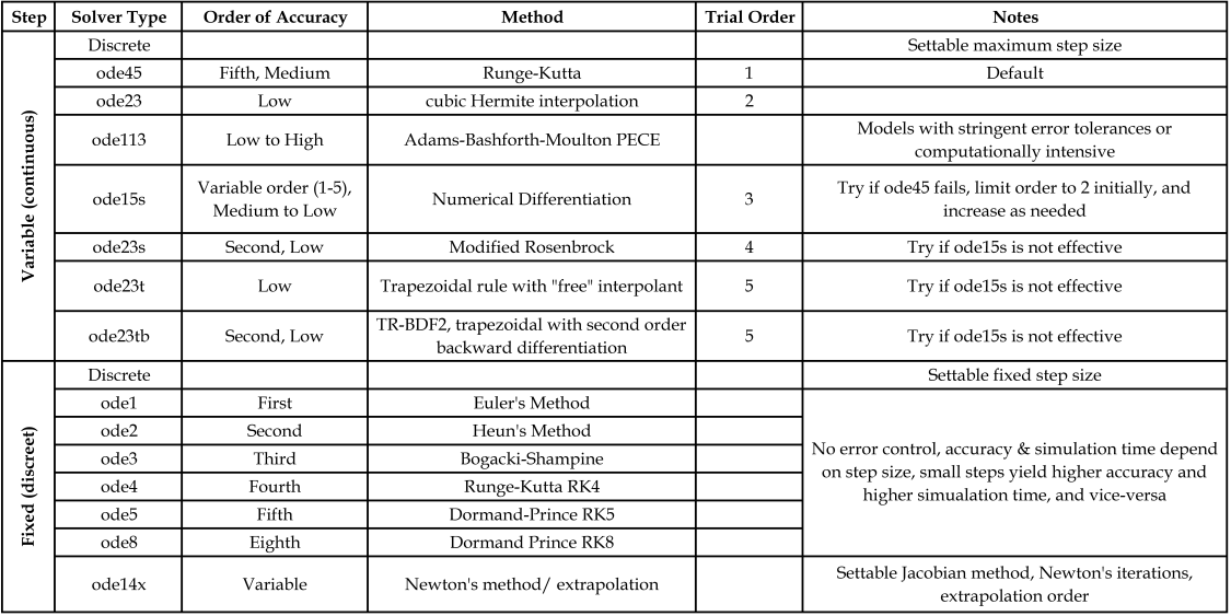
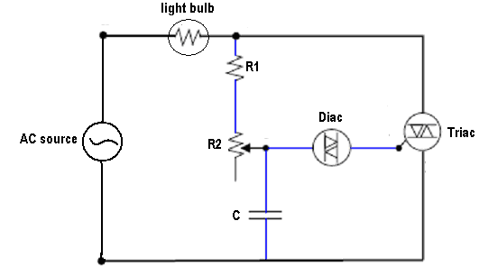
Fig. 1 depicts the circuit configuration for a simple light dimmer where the primary power control device is the Triac whose gate firing device is the Diac (Skvarenina, 2002). The Diac is a fixed break-over voltage device compared to the Triac that permits a variable firing angle through its gate terminal. Compared to the Silicon Controlled rectifier (SCR) which is also gate controlled, the Triac permits device firing on the positive and negative half-cycles of the AC waveform. The SCR has a similar characteristic to that of a rectifier (unidirectional) but with an adjustable conduction angle (Rashid, 2004). Both devices are self-commutated, i.e. they turn off naturally at the zero crossings of the waveform. The triggering circuit for the Triac is comprised of R1, R2, and C where the potentiometer R2 represents the adjustable resistor which is usually operated by the dial (or slide switch) on the operating plate of the light dimmer. The value of R2 controls the conduction phase of the Triac. As the capacitor charges to a voltage higher than the break-over voltage of the Diac, a pulse is produced at the gate of the Triac to turn it on. In the conduction mode, the internal resistance of the Triac becomes small causing the flow of current through the light bulb. A higher value of R2 elongates the charging time of C (longer time constant τ=C(R1+R2)), causing a delayed triggering pulse and a shorter conduction period for the Triac. The average power transmitted to the light bulb becomes less, resulting in a dimmer light. The same logic works for both halves of the source’s waveform cycle. This application will be analyzed using Matlab in Section 4 to demonstrate some of the capabilities of the SimPower and Simulink tool boxes.
MATLAB – A Fundamental Tool for Scientific Computing and Engineering Applications – Volume 1
Figure 1. Light Dimmer Circuit
Several practical notes relative to the circuit in Fig. 1 are due, 1. While it may seem that the Diac is an unnecessary device in this application since the voltage of the capacitor may trigger the gate of the Triac directly, it must be noticed that Triacs are notorious for not firing symmetrically. Lack of symmetry in triggering at the same voltage level for both polarities of a full cycle produces unnecessary additional harmonics that negatively affect the efficiency of the circuit. The symmetrical characteristic if the Diac provides accurate timing that enhances the firing symmetry of the Triac.
2. One may use two SCRs back-to-back to implement the power control device in place of the Triac.
3. The firing time through the RC circuit is perfectly synchronized with the conduction cycle of the Triac because they are both powered by the same AC source.
2.2. Dc-Dc Converter
Converting DC voltage to the proper levels from a single energy source that might be depleting, like in battery applications, requires employing energy storage elements (inductors) with associated power electronics devices. When switched ON-OFF at a certain rate, stored energy gets released to the load at the proper time to maintain the desired voltage level. Pulse-Width-Modulation (PWM) techniques are most popular in this application. Converters of this type are suited for boosting or bucking the source voltage; commonly known as switching power supplies. Since the current is DC and zero crossing is not one of the steady cyclic features like in AC circuits, self-commutation is not possible.
Therefore, Gate-Turn-Off (GTO) devices are required (Skvarenina, 2002). These devices are turned off with a negative pulse on the gate terminal. MOSFETs and BJTs also provide a viable option in low power applications. Feedback loop methodologies are an integral part of DC-DC converters to regulate the load voltage, compensating for load variations and irregularities in the source voltage.
Current and voltage ripples, and high frequency harmonic distortion are common byproducts of switching techniques. Capacitors are usually employed to insure acceptable ripple content. Harmonics negatively affect the efficiency of the converter and produce Modelling and Characterization of Power Electronics Converters Using Matlab Tools 137 losses in the form of heat. While the produced load current is regulated for a desired average value, the cyclic behavior produces current fluctuations in the energy storage elements. Operating at zero current for energy storage elements during part of the cycle results in a highly nonlinear characteristic, where the converter is known to be in its Discontinuous Conduction Mode (DCM). The Continuous Conduction Mode (CCM), however, insures nonzero current during the full cycle of switching (Rashid, 2004; Shaffer, 2007). Each mode of operation has certain implications on the ripples and harmonics content which affects the efficiency of the converter.
2.2.1. Buck Converter
In low power applications, voltage bucking is usually achieved using voltage divider resistors. This simple solution is acceptable because the current is usually too small to cause significant losses in the resistors. Employing this approach in high power applications is unrealistic because the losses of the resistors may exceed the useful power consumed by the load; that is in addition to the associated heat dissipation issues that must be resolved to insure sufficient ventilation. The DC-DC converter provides a more practical solution in spite of its associated design complexities at times.
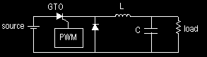
Bucking DC source voltages can be achieved using a topology like the one shown in Fig. 2. The energy storage element (L) is to be sized for the desired mode of operation (CCM or DCM). The power device (GTO in this case) switches On-OFF using PWM where the duty- ratio (D=Ton/T) determines the average load voltage; T is the time of one period of the switching frequency (f). The diode facilitates inductor current wheeling during the OFF time of the GTO. The capacitor is usually sized to reduce the load current ripples. The inherent inductor current ripples (usually in the range of about 30%) are then facilitated by the capacitor while blocking it from flowing through the load. Snubber circuits are installed across the power devices for protection and to minimize the stress on the device that may result from opening the circuit while the current cannot be stopped instantaneously due to the nature of the energy storage element. Current and voltage waveforms will be shown in Section 4 for illustration.
Figure 2. Dc-Dc Buck Converter
Design of the DC-DC converter centers around determining the size of the energy storage element (L) which achieves predetermined Vsource, Vload, ∆Vload (load voltage ripple), and Iripple. Knowing that Iripple=∆IL, D=Vload/Vsource assuming CCM, T=1/f, and VL=Vsource-Vload during Ton (Rashid, 2004), Eq. (2) can be obtained.
(2)
Notice that L is charging during Ton only, which means that ∆T=D/f. The calculated “L” is usually well above the minimum inductance needed to insure CCM in many applications. Only very light load conditions may force DCM.
The capacitor “C” is sized to reduce load current ripple while providing a pass for the inductor current ripples (Iripple). It is worth noting that the inherent Effective Series Resistance (ESR) of the capacitor plays a major role in determining the size of the capacitor.
(5)
Eq. (5) shows that the capacitor’s ESR rating can have a significant effect on the size of the capacitor knowing that the tolerated ∆Vload is usually small in sophisticated applications. Therefore, the ESR rating shouldn’t be overlooked when selecting the capacitor. The Effective Series Inductance (ESL) rating of the capacitor is also relevant but it is usually considered for very high switching frequencies only (>1 MHz). By then, inductive effect of board tracings can start to be critical as well.
Modelling and Characterization of Power Electronics Converters Using Matlab Tools 139
2.2.2. Boost Converter
While bucking the source voltage for low power applications can be achieved with resistor voltage dividers (passive components), boosting the voltage requires active devices like Operations-Amplifiers (OpAmps). Power OpAmps are also available for low-voltage medium power (500 Watt) applications but they usually exhibit high power loss and they need active cooling (fans) in addition to passive cooling via heat sinks. OpAmps are also analog devices which are usually controlled with analog control voltages, while PWM controlled power devices can be easily interfaced with digital controllers. Real-time load voltage regulation is achieved most effectively with embedded digital controllers.
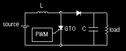
By rearranging the components of the buck converter as shown in Fig. 3, it becomes possible to boost the source voltage. The underlying principle of operation is in the fact that the polarity of the inductor (L) voltage reverses instantaneously when the rate of change in the inductor current (iL) reverses pattern; i.e. diL/dt changes sign. During the ON time (Ton) of the GTO, the inductor charges with its voltage taking the opposite polarity of the source.
When the GTO turns OFF during Toff, the inductor current starts to drop and accordingly its polarity reverses direction to become in the same direction like the source. The load, then, becomes supported by Vsource plus VL which signifies the higher load voltage compared to the source voltage. The role of the capacitor is similar to that of the buck converter, that is to reduce the ripples of the load voltage as it supports the load voltage during Ton in this case.
It must be noted that VL is equal to L(diL/dt) which means that the inductor voltage can rise significantly if the current is allowed to change at a high rate, resulting in load voltages much higher than that of the source. The inductor, however, must be sized properly and allowed to charge enough by increasing the duty-ratio (D) of the PWM scheme such that it stores enough energy to feed the load during Toff. The ratio Vload/Vsource is determined by 1/(1- D) which implies that Vload can rise well above Vsource as the duty ratios gets closer to 100% (Rashid, 2004). The physical limit of the employed components is usually the determining factor for how high Vload may be attained.
2.2.3. Buck-Boost Converter
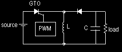
Rearranging the components as shown in Fig. 4 provides the flexibility to buck or boost the source voltage by adjusting the duty-ratio (D) of the PWM. A 50% duty-ratio provides the load with the same source voltage while a lower duty-ratio bucks the voltage and a higher duty ratio boosts the voltage (Rashid, 2004). It was proven that Vload/Vsource is determined by MATLAB – A Fundamental Tool for Scientific Computing and Engineering Applications – Volume 1
140
D/(1-D). The orientation of the diode is such that the load current is blocked while the inductor is charging during Ton. During Toff the inductor releases its energy to the load through the diode loop resulting in an opposite voltage polarity compared to that of the buck or boost configurations. The size of the storage element (L) is critical to facilitating the boost mode. To insure CCM, the inductor must be of a certain minimum size (Rashid, 2004).
Current and voltage waveforms will be shown in Section 4 for illustration.
2.3. Voltage Control
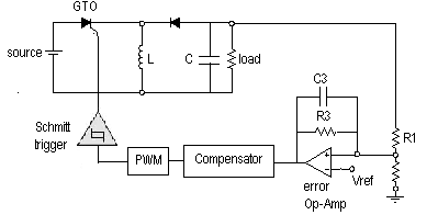
Control of switching power converters requires modulating the width of the pulse provided to the power devices’ gate, based on feedback from the load voltage and the inductor’s current. Fig. 5 illustrates the basic components of an analog control scheme; where the output voltage provides the desired feedback. This scheme is identified as the “voltage- mode” control. The low-pass filter (R3, C3) of the error amplifier along with R1 provide feedback gain and reduce harmonics. The PWM hardware can be a typical controllable IC and the Schmitt-trigger is to produce sharp edges for the power device’s gate. Needed high gate current usually requires current amplification as well.
The compensator can be implemented with Op-Amps to realize desired dynamic characteristics for voltage recovery and regulation. Traditional compensators like PID, lead- lag, and Sliding Mode Control (SMC) are all applicable. Digital control, however, provides flexibility in implementing sophisticated control schemes and mixed mode operations to achieve power saving and to possibly automatic controller tuning. Digital schemes also reduce magnetic interference effects which would most probably exist in applications that require DC-DC power conversion. Digital Signal Processors (DSPs), microcontrollers, and Field Programmable Gate Arrays (FPGAs) together with the Analog-to-Digital Converter (ADC) are widely used to implement digital controllers. However, high-speed high- resolution ADCs are expensive and they are not easy to consolidate into an integrated circuit.
Design of the compensator requires transient analysis and solving the differential equations that describe each waveform. Retaining the instantaneous detailed characteristic of the circuit requires analysis of each mode of the switching cycle. This level of detail is usually not necessary for the design of the compensator. Averaging over a number of switching cycles provides viable approximate models (Forsyth & Mollov, 1998) which simplify the compensator design significantly. In this technique, the state equations for the RC circuit are Modelling and Characterization of Power Electronics Converters Using Matlab Tools 141 written for both modes of the converter (ON and OFF). A combined state equations model is then formed using the weighted average of the state matrices of the ON and OFF models according to the duty ratio (D). The produced model is a set of two linear time-variant state equations which ignore ripple components. The time-variant effect is due to the presence of the control variable “D(t)” (varying duty-ratio) in the state matrices rather than being part of the input control variables vector. Since solving time-variant equations is difficult, further simplifications are required. Linearization techniques are then employed for specific operating conditions, resulting in small-signal state-space models (Johansson, 2004). These models facilitate frequency and time domain design methodologies.
Figure 5. Voltage Control Of Buck-Boost Converter
In addition to the above explained voltage-mode control scheme, current-mode control can also be achieved by sensing the current of the switching power device or the energy storage element and integrating it into the main voltage control loop (Johansson, 2004). In this scheme, the output of the voltage compensator acts are the reference voltage for the current feedback loop which controls the PWM and adjusts the gate pulse for the power device. This scheme usually improves the stability of the converter in high performance applications.
Controlling the peak inductor current is one of the popular schemes employed. Current sensing can also be used to determine when to switch between CCM and DCM which facilitates implementing high efficiency schemes for operation.
2.4. Power Saving And Improved Efficiency
Minimization of DC-DC converter power losses is important to accommodate the growing need for a longer battery life and reduced size and weight of portable electronic devices. Power losses are usually dependent on the type of power devices and their conduction losses, the effective series resistance of inductors and capacitors, mode of operation of the converter, switching scheme, and the switching frequency. While diodes are simple in their use, they may reduce the efficiency of the converter due to their high losses in certain modes of operation. The same function of a diode can be achieved by using a switching power device similar to the main energy transfer device of the converter (e.g. GTO or MOSFET).
142
This will require applying switching logic to multiple devices in the same converter. Synchronizing the switching of the devices introduces an additional control challenge and the converter topology is therefore referred to as the “synchronous” topology. The diode topology is then called “asynchronous”. A detailed characterization of power losses in DC- DC converters is offered by Gildersleeve, et.al., (2002).
Various techniques were proposed in the literature to reduce power losses in DC-DC converters, including soft-switching (Zhou & Rincon-Mora, 2006), synchronous rectification (Djekic & Brkovic, 1997; Arbetter et al., 1995), mode hopping between CCM and DCM (Wang et al., 1997), Zero-Voltage Switching (Stratakos, 1998), mixed synchronous- asynchronous control (Saggini et al., 2007), variable switching frequency (Djekic & Brkovic, 1997; Arbetter et al., 1995), and Hybrid Mode Hopping combined with variable frequency (Wang et al., 1997). These techniques are summarized and compared by Zhou (2003). Djekic et al. (1997) compared synchronous and asynchronous rectification buck converters for efficiency at various loads and switching frequencies. This work was extended to the buck- boost converter recently (Fagerstrom & Bengiamin, 2011). The methodologies herein build on that latest work.
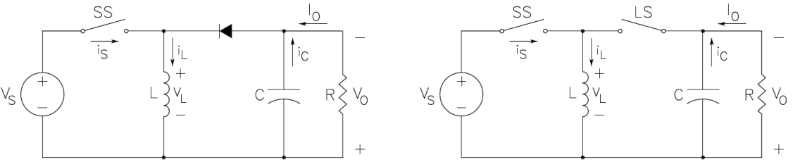
The basic asynchronous and synchronous converter topologies are given in Figs. 6.a and 6.b, respectively. Table 1 lists the sources of losses considered assuming a MOS switching device.
(B) Synchronous
Modelling and Characterization of Power Electronics Converters Using Matlab Tools 143 Extensive lists of DC-DC converter losses may be found in Zhou, S. (2003) and Djeki, O. & Brkovic, M. (1974). Buck-boost converter losses considered in this work are given in Table 1, as itemized and developed analytically in the following subsections. The PMOS is used for the Source Switch (SS) and NMOS is used for the Load Switch (LS), respectively.
a.
Pmos Source Switch Conduction Loss
When the PMOS transistor is in forward conduction there is a resistive loss in accordance with Eq.(6). PMOS conduction loss is associated with both asynchronous and synchronous converters (Gildersleeve et al, 2002; Klien, J., 2006).
(6)
Where, ISS=PMOS current (Amp) RDS=PMOS forward conduction ON resistance (Ohm),
D=Duty Ratio
b.
Pmos Source Switch Switching Loss
During the transition of voltage rising or falling between the maximum and minimum steady-state values across either switch, and similarly the rise or fall transition of current through the same switch, losses occur. Much work has been done in an effort to correctly model this behavior (Klein, 2006; Xiong et al, 2009), without a highly accurate model still as yet developed. A combination of the work of Klein, (2006) and Xiong et al, (2009) are presented here to develop the switch model loss. The development starts with the following power loss equation.
(7)
Where, PSW=MOSFET switching loss power (Watt), ISW=current through MOSFET (Amp), VSW=drain to source voltage across the MOSFET, fs=switching frequency (Hertz),
Time
transitioning on. All parameters of Eq. (7) are readily measurable in a physical circuit except the switching time terms toff and ton which are developed in the following equations.
(12)
Where, QG(SW)=MOSFET switching-point gate charge (Coulomb), IDriver(L-H)=MOSFET gate current while switching on (Amp), IDriver(H-L)=MOSFET gate current while switching off, VDD=gate drive controller voltage, VSP=MOSFET gate voltage at switching point, RDriver(Pull- up)=gate drive controller internal resistance, RG=MOSFET gate resistance, VG=MOSFET gate switching voltage, Gm=MOSFET transconductance.
Combining Eqs. (7) through (12) gives the combined switching loss Eq. (13).
(13)
c.
Pmos Source Switch Gate Drive Loss
Gate drive loss accounts for the energy dissipated by the MOSFET to drive the gate for the switching operation. The loss equation is given in Eq. (14). PMOS gate drive loss is associated with both converters.
(14)
d.
Nmos Load Switch Conduction Loss
Load switch conduction loss is similar to that of the source switch shown in Eq. (6), differing by the (1-D) factor as this loss occurs during the latter portion of the switching period. This loss is represented in Eq. (15). NMOS conduction loss is associated with only the synchronous converter.
(15)
Where, ILS=load switch drain to source voltage. e.
Nmos Load Switch Switching Loss
The load switch MOSFET switching loss is calculated with the same model as the source switch shown in Eq. (14). NMOS switching loss is associated with only the synchronous converter.
f.
Nmos Load Switch Gate Drive Loss
NMOS gate drive loss is accounted for by simply doubling the gate drive loss Eq. (15) for the synchronous case. NMOS gate drive loss is associated with only the synchronous converter.
Modelling and Characterization of Power Electronics Converters Using Matlab Tools 145 g.
Nmos Load Switch Body Diode Loss
The load switch body diode loss occurs only in the load switch due to the reverse bias during the ON portion of the period (Djekic et al., 1997). The reverse-bias voltage and leakage current dissipate power according to the equation shown in Eq. (16). NMOS body diode loss is associated with only the synchronous converter.
(16)
Where, ileakage=reverse bias leakage current, VLS=load switch drain to source voltage. h.
Synchronous Switching Dead-Time Loss
Dead-time loss occurs through the load switch when neither transistor is on as the load switch is in forward conduction (Klien, 2006). A period of dead-time must exist to prevent current “shoot-through” whereby current flows through both switches simultaneously to the load. The value of tdead is assumed to be 60 ns as is typical for DC-DC converter controllers (Djekic & Brkovic, 1997). The dead-time loss representation is shown in Eq. (17).
Synchronous switching dead-time loss is associated with only the synchronous converter.
(17)
Where, Iload=load current, tdead=time where both switches are off. i.
Diode Conduction Loss
Diode forward conduction losses are found with the equation shown in Eq. (18). Diode conduction loss is associated with only the asynchronous converter.
(18)
Where, ID=current through diode, Vf=diode forward voltage. j.
Diode Reverse Bias Loss
During the portion of the period d, the diode has a reverse bias across it. There is a certain amount of leakage current under this condition that is listed by the manufacturer on the data sheet. This value is used to calculate diode reverse bias leakage loss in Eq. (19). Diode reverse bias loss is associated with only the asynchronous converter.
(19)
Where, VD=voltage across diode. k.
Diode Junction Capacitance Loss
Diodes have a certain capacitance associated with changing voltages across them (Klein, J., 2006). The charging and discharging of this capacitance creates a power loss as modeled by Eq. (20). Diode junction capacitance loss is associated with only the asynchronous converter.
3. Matlab Capabilities
The Matlab simulation platform (by MathWorks, Inc.) offers a versatile and robust option in design and simulation of power electronic converter systems. Matlab is matrix based, offering diverse options in data manipulation, preparation, and presentation. Simulink, a sub-program of Matlab included in the standard software package, offers a relatively high-level programming language utilizing drag-and-drop function blocks that mask embedded functions. These icons can be incorporated into yet larger models and again masked into new system blocks. This modular block-symbol based modeling system allows ease of construction and programming of large complex systems while maintaining the ability to edit and control internal systems all the way down to the most base-level functions.
The power electronic system designer upon starting Simulink, then, is entering the design process at the phase of assembly of power electronic, measurement, and signal routing components into larger more complex systems to accomplish a desired task. The designer may from time to time wish to delve into base Simulink models to change component characteristics and behavior, add base-level monitoring of characteristics, change signal routing, confirm calculation methods, or even develop system models from scratch.
This section is intended for the Matlab user who possesses basic workspace programming knowledge. Many resources are available to learn or refresh on Matlab workspace programming, including the help files included with the Matlab software. Matlab help files are an invaluable resource in workspace and Simulink programming and are recommended for perusal.
3.1. Simpowersystems Toolbox
Simulink provides a rich suite of toolboxes applicable to wide areas in engineering applications. The power electronics devices discussed in this chapter are simulated using “SimPowerSystems”, a versatile toolbox for modeling electro-mechanical systems. In addition to popular power electronics devices, this toolbox provides a wide range of simulation apparatuses such as transformers, rotating machines, hydraulic turbine & governor, and wind turbines, as well as basic electric circuit components. Detailed characteristic parameters can be configured for these components to represent typical performance scenarios. To monitor the performance of constructed models, a host of measurement blocks are available for discreet, continuous, and phasor based measurements.
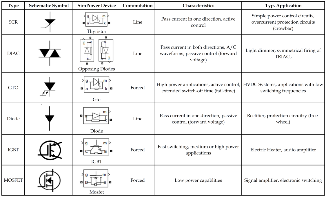
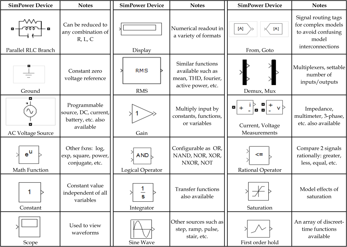
Relevant variables like active & reactive power, total harmonic distortion, and power factor can be monitored with ease. Custom functions can also be set up with simple manipulations. Since this chapter deals with power electronics applications, attention is focused on the Power Electronics block-set which includes several power electronics semiconductor Modelling and Characterization of Power Electronics Converters Using Matlab Tools 147 simulation blocks relevant to industry, Table 2. Devices shown in Table 2 are modeled into systems with other standard Simulink and SimPower devices, some of which are presented in Table 3.
3.2. Simulation Parameters And Data Presentation
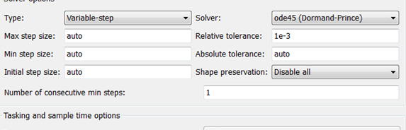
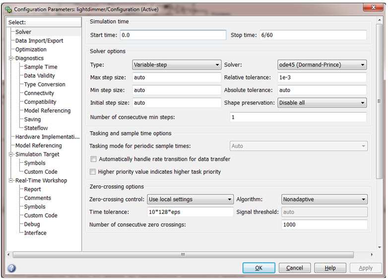
For proper numerical computations Matlab provides various simulation options including the specific numerical method (solver), the allowed tolerance, and mode of computation. Since some numerical methods are more computationally intensive than others, the user may choose a less intensive method for simulations that don’t require solving highly nonlinear differential equations, for example. This improves the efficiency of the simulation and accelerates obtaining results. Some trial and error may be necessary to achieve a successful simulation. However, the default simulation options can typically be used for most simulations. If the simulation takes too long to execute or the computed data is incomplete, is at an unacceptable resolution, or has errors, it will be necessary to change simulation parameters. Highly complex simulations may require some time invested in finding the correct solver for the application in order to achieve a good balance between accuracy and computation times. The Configuration Parameters dialog box is found under the Simulation tab in Simulink, Fig. 7. Usually the best choice is to leave these set to “auto” to allow Simulink to determine simulation parameters automatically, based on the model.
C
Modelling and Characterization of Power Electronics Converters Using Matlab Tools 149 The solvers are categorized into two general types: Fixed step, and Variable step. Fixed step simulations evaluate in user-set time steps that are constant throughout simulation. Variable step solvers dynamically change the simulation step size to optimize simulation time vs.
accuracy. Therefore, the goal in choosing the solver is to find the least computationally intensive method that yields the level of accuracy required. Solver types are summarized in Table 4.
3.3. Configuration Of Simpowersystems Blocks
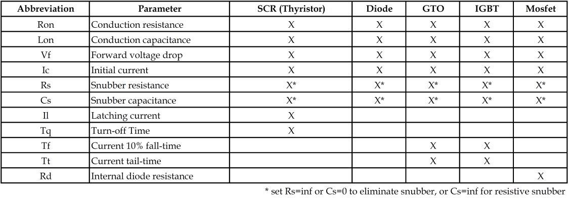
Simulation of any SimPower circuit involves parameter configuration within model blocks after circuit is constructed. This is achieved by double-clicking on the circuit block to reveal block parameters. Table 5 shows the possible block configuration parameters for common SimPower power electronic devices. A user may also elect to use typical values provided by default.
Table 5. SimPowerSystems Block Configuration Parameters
Deployment In Out-Of-Position Situations
D. Bendjaballah1, A. Bouchoucha1, M. L. Sahli1,2* and J-C. Gelin2
Abstract
Side-impact collisions represent the second greatest cause of fatality in motor vehicle accidents. Side-impact airbags have been installed in recent model year vehicle due to its effectiveness in reducing passengers’ injuries and fatality rates. In meeting these requirements, simulations of folding and deploying airbags are very useful and are widely used. The paper presents a simulation method for the deploying airbags using three materials in different working conditions. Finite element analysis is primarily used to evaluate this concept. In these simulations, the gas flow is described by the conservation laws of mass, momentum, and energy. The numerical results indicate that the FE method in this paper is capable of capturing airbag deploying process accurately.

Keywords: Airbag simulations, Out-of-position, Crash, Modeling, Out-of-position
Background
The passive safety of cars has become a very high prior- ity issue for the automotive industry. Today, there are not only one or two airbags in a car; certain models have ten times more than that. With the increasing usage of airbags, the number of accidents where the airbag itself can cause an injury to the occupant also increases
(Augenstein Et Al. 2003; Gabauer And Gabler 2010;
Audrey et al. 2011). As is well known, safety belts are also now devices designed to provide protection to the users of vehicles during crash events, minimizing the loads necessary to adapt their movement to the move- ment of the car (Freesmeier and Butler 1999; Schmitt et al. 1997). In general, the seat belt is designed to restrain the occupant in the vehicle and prevent the
Occupant From Having Harsh Contacts With Interior
surfaces of the vehicles. The airbag acts to cushion any impact with vehicle structure and has positive internal pressure, which can exert distributed restraining forces over the head and face. As a safety component of auto- mobile, an airbag decreases occupants’ injury likelihood effectively in case of an accident (Ruff et al. 2007). These safety elements can reduce the death rates on the roads, and its protection effects have been widely approved (Crandall et al. 2001; Teru and Ishikawa 2003). With computational tools such as finite element methods designed for dynamic contact problems, crashworthiness simulations can now be used with reliable accuracy to evaluate occupant protection in various collision condi- tions with safety metric/parameters such as acceleration, head injury criteria, intrusion distance, intrusion vel- ocity, and neck forces (neck injury risk or whiplash).

Thus, new types of airbag products are being developed to handle different collision scenarios.
Become Standard Equipment On Most New Passenger
vehicles (Braver and Kyrychenko 2004; Teng et al. 2007; Yoganandan et al. 2007). The airbag cushion is com- posed of a woven fabric which is rapidly inflated during a car crash. The airbag dissipates the passenger’s kinetic energy thereby reducing injury through biaxial stretching of the fabric bag and escaping gas through vents. There- fore, the performance of the airbag is greatly influenced by the mechanical properties of the fabric. Generally, air bags are designed to deploy in a crash that is equivalent to a vehicle crashing into a solid wall at 8 to 14 mph.
Air bags most often deploy when a vehicle collides with another vehicle or with a solid object like a tree. There are various types of airbags: frontal, side-impact, and curtain airbags. In general, the passenger side airbags are usually larger than the driver airbags (see Fig. 1).

Besançon, France
© The Author(s). 2017 Open Access This article is distributed under the terms of the Creative Commons Attribution 4.0 International License (http://creativecommons.org/licenses/by/4.0/), which permits unrestricted use, distribution, and reproduction in any medium, provided you give appropriate credit to the original author(s) and the source, provide a link to the Creative Commons license, and indicate if changes were made.

Bendjaballah et al. International Journal of Mechanical
Doi 10.1186/S40712-016-0070-2
Extensive studies have shown that the airbag deploy- ment in load cases consists of two occupant loading phases: a punch-out effect where the airbag bursts out of its container with the airbag and airbag module cover accelerating towards the occupant and a second loading phase during which the airbag is taking on its deployed shape and volume (membrane-loading effect). Bankdak et al. (2002) developed an experimental airbag test system to study airbag-occupant interactions during close proximity deployment. The results provided insight for simulating the effect of inflation energy and mass flow on target response. Bedard et al. (2002) found that while left-side (driver-side) impacts accounted for only 13.5% of all crashes, the fatality rate among these
Crashes Was 68.3% In Comparison To Front Impact
(48.3%), right-side impact (31.3%), and rear impact (38.4%). These studies underscore the importance of oc- cupant safety during side-impact collisions. In the last years, the current market requested to reduce the time and cost airbag development. In order to achieve this result, virtual simulations play an important role since they allow to minimize the number of experimental tests (Pei et al. 2013; Cao et al. 2014). Several simulation models of airbag were established (Wang et al. 2007). It is feasible to optimize the parameters of airbag deploy- ment using simulation technology. Experimental and numerical studies have quantified injury risks to close- proximity occupants from deploying side airbags. These studies have focused on the prevention of the most ad- verse effects of airbag deployment (Duma et al. 2003).
Other studies have proposed airbag characteristics to minimize particular biomechanical responses (Haland and Pipkorn 1996). In a more recent study, Marklund and Nilsson (2003) compared deformation patterns with experimental data as well as the computational costs associated with three different airbag deployment simu- lation methods; they concluded that the SPH method is relatively inexpensive and produces incremental deform- ation patterns that compare most closely to the experi- mental results. The process of inflation of an airbag is one of the determining factors in saving lives. The duration from the initial impact of the crash to the full inflation of an airbag is about 40 ms, and during this time, the airbag goes from being in a folded state to a fully inflated state, with a high internal pressure. After achieving this state, the airbag begins to deflate, thus providing a nice cushion for the body impacting it.
Ideally, the person in the crash should come into contact with the airbag at this time. In the present study, a large volume passenger side airbag model is developed to handle different collision scenarios. The main aim is evaluate the performance of deploying of passenger side airbag using finite element methods (FEM).
Materials
The tensile specimens were made in different airbags (P: Peugeot, R: Renault, and VW: Volkswagen) with a length of 200 mm long and a width of 40 mm. Table 1 shows the mechanical properties of the airbag.
Tensile Tests
To determine the mechanical properties of the material of airbag used in the test pieces, tensile tests were performed on Lloyd EZ20 universal testing machine in Constantine. These tests were conducted using rect- angular samples. The axial force and axial displacement acquired during a test are converted into stress and the strain in order to be used for the fabric material model.
The continuous recording of the stress-strain data was performed during both the load and unload phases. A minimum of five samples were made in order to check the repeatability of the measurements. All the data was collected by using a PC-based data acquisition system and analyzed by commercial software. The picture frame test device that is made for this study is shown in Fig. 2.
Fig. 1 a Frontal and side airbags. b Oblique view of facet occupant model in sitting posture following airbag deployment (Lim et al. 2014)
0.150
Bendjaballah et al. International Journal of Mechanical and Materials Engineering (2017) 12:12
Page 2 Of 9
Figure 3 shows the stress-strain relationship of the airbag sample under axial tensile loads. The results are showing a linear increase in extension with the increas- ing stresses. This is an expected output and it confirms with the theoretical behavior of a sample subjected to tensile stress. The rupture strain values for different airbags (R/P/VW) were 0.322, 0.441, and 0.472, respect- ively. The measured elastic parameters (i.e., Young’s modulus E and initial yield strength) and Poisson’s ratio are summarized in Table 2. The tensile tests of the woven fabrics can show differences on mechanical prop- erties because woven fabrics can resist in-plane shear loads once the yarn lock-up angle has been reached. The differences of material property on material direction can affect the shape of fully deployed bag (see Fig. 3b).
Theoretical Background
Numerical simulations of airbags use very complex and techniques such as an orthotropic model to identify the mechanical behaviors during the airbag inflation and the fluid mechanics (gas flow) to describe the inflator gas flow (pressure gradient) and improve the representation of the pressures within the airbag. To model the airbag as an orthotropic model, three material constants have to be provided. Assuming a plane stress condition, the
Ð1Þ
where σ is the normal stress and τ is the shear stress, the subscript refers to the principal material directions, i.e., the fill and warp directions. Also, ε and γ are the strain components. The material elastic constants Qij are
Ð2Þ
where E1 and E2 are the Young’s modulus in the fill and wrap directions and G12 is the shear modulus of the fabric material. νij is the Poisson ratio of the material.
The gas exerts a pressure load on the airbag causing it to expand. This expansion puts the airbag under tensile stress lowering the expansion rate. In this study, heat conduction and heat transfer is not taken into account.
Fig. 2 A photograph of Lloyd EZ20 universal testing Fig. 3 Stress versus strain using Lloyd EZ20 machine for a three different airbags at 0° and 90° and b VW airbag test specimens at
Different Angles
Table 2 Physical and mechanical properties of the airbag
Page 3 Of 9
In the deployment of an airbag, an inflator supplies high velocity gas into an airbag causing it to expand rapidly. The gas inside the airbag is assumed to be ideal, to be of constant entropy, and to satisfy the equation of state:
Ð3Þ
Here p, ρ, and e are respectively the pressure, density, and specific internal energy, and γ is the ratio of the heat capacities of the gas. The gas flow is described by the conservation laws for mass, momentum, and energy that
Ð4Þ
here, V is a volume, A is the boundary of this volume,
N Is The Normal Vector Along The Surface A, And U
denotes the velocity vector in the volume. Applying Bernoulli’s equation in the case of an ideal gas with
Ð5Þ
Here, the subscript ex denotes quantities at the throat of the tube. Furthermore u, p, and ρ denote the quan- tities inside that part of the tube that is supplying mass.
Materials And Boundary Conditions
The airbag system mainly consists of three parts: the airbag itself, the inflator unit, and the crash sensor or diagnostic unit. Thus, to study the behavior of the airbag using FE simulations, we need to have an FE model of the airbag in the folded position. A FE model of the airbag was used to simulate the test condition as shown in Fig. 5. LS-DYNA® material model FABRIC (MAT_34) is used to simulate the airbag material. It is a variation of the layered orthotropic material model. Additionally, in the LS-DYNA® material model, fabric leakage can be accounted for. However, for this CAB material, the leak- age is almost negligible and therefore no leakage is specified. The mechanical properties can be determined from the physical test. Typical material properties for airbag fabrics are taken as given in Chawla et al. (2004a) (Table 3). These properties are used to simulate inflation process of airbag (see Table 1). The car dashboard is modeled as the rectangular thin plate using a MAT_RI-
Gid Material, And The Degrees Of Freedom Are Con-
strained in all the directions. The similar properties of thermoplastic polymer are assigned for contact purposes. The porosity of the fabric is assumed zero. The nitro- gen gas is taken for inflating the airbag. Properties of nitrogen gas and initial bag conditions are shown in Table 4. The example on which we perform the study is a typical passenger side airbag. The geometric de- tails have been measured from a commercially avail- able airbag. The initial state of the airbag is a closed rectangular whose sides are to be finished to 482 × 635 mm2 and is shown in Fig. 4.
Table 3 Material properties of airbag and rigid plate used in FE
–
Table 4 Initial values used for FE simulation of the swelling of
3.33 × 10⁻⁴
Fig. 4 The initial airbag geometry in the form of a rectangular Bendjaballah et al. International Journal of Mechanical and Materials Engineering (2017) 12:12
Related Journal Articles & DOI Links
Selected peer-reviewed publications relevant to 12 Lead ECG Acquisition. Click the DOI to access the full paper (may require institutional access).
-
1. Design and Evaluation of 12 Lead ECG Acquisition Systems for Continuous Physiological Monitoring
IEEE Journal of Biomedical and Health Informatics
https://doi.org/10.1109/JBHI.2020.2981234 -
2. Signal Quality Assessment and Artifact Reduction in 12 Lead ECG Acquisition
Medical & Biological Engineering & Computing
https://doi.org/10.1007/s11517-020-02145-6 -
3. Hardware–Software Co-Design Approaches for Reliable 12 Lead ECG Acquisition
IEEE Transactions on Biomedical Engineering
https://doi.org/10.1109/TBME.2019.2895762 -
4. Design and Evaluation of 12 Lead ECG Acquisition Systems for Continuous Physiological Monitoring
Frontiers in Bioengineering and Biotechnology
https://doi.org/10.3389/fbioe.2020.00123 -
5. Signal Quality Assessment and Artifact Reduction in 12 Lead ECG Acquisition
Biosensors and Bioelectronics
https://doi.org/10.1016/j.bios.2021.112345 -
6. Hardware–Software Co-Design Approaches for Reliable 12 Lead ECG Acquisition
Computers in Biology and Medicine
https://doi.org/10.1016/j.compbiomed.2021.104567 -
7. Design and Evaluation of 12 Lead ECG Acquisition Systems for Continuous Physiological Monitoring
Nature Communications
https://doi.org/10.1038/s41467-020-12345-6
Why Choose Us?
Bangalore guidance for robotics, Spectre and autonomous systems projects.
Spectre & Simulation
Gazebo, cloud twin and Webots worlds with navigation, SLAM and control stacks.
Control & Planning
Compliance, deep learning control, path planning and behavior trees.
Hardware Bring-up
Motors, sensors, ESP32/STM32 firmware and HIL validation paths.
Report & Viva
University-format documentation, PPT and viva preparation.
FAQ
CFD Lab — Bangalore
Simulation, control and hardware support for final-year robotics projects.
Stacks
Worlds
Digital Twin
Control
Robots
Offline
Bring-up