PWM Generation Using FPGA — Tools & Flow
Configurable PWM generator with duty cycle, frequency control, optional dead-time insertion and FPGA output verification.
Typical stack: Verilog/SystemVerilog, ModelSim/Questa, Xilinx/AMD Vivado or Intel Quartus, FPGA boards (Basys3, Nexys, DE10), synthesis timing/area/power reports.
Tools & Hardware
Abstract
This project presents a practical study of PWM Generation Using FPGA, with emphasis on the architecture, RTL/logic behaviour, verification flow and implementation considerations. The design is organized into clear functional blocks so that the input conditions, internal processing and output response can be observed and validated systematically. The project is suitable for VLSI, FPGA and digital-design laboratory work where a reproducible simulation and implementation flow is required.
The proposed workflow starts from functional specifications and block-level design, followed by HDL modelling, testbench development and functional simulation. For this topic, AMD Vivado is used as the primary design or analysis environment, while ModelSim / QuestaSim can be used for waveform-oriented verification where applicable. Important parameters such as latency, throughput, resource usage, timing behaviour, switching activity or signal integrity are examined according to the nature of the design.
After simulation, the design can be synthesized and mapped to a Xilinx Zynq-7000 FPGA for practical demonstration when the selected architecture is FPGA-compatible. The implementation stage can include pin assignment, clock constraints, synthesis reports, implementation reports and on-board I/O validation. This creates a useful connection between the theoretical design, simulation waveforms and real programmable-hardware behaviour.
The expected project outputs include the HDL source files, testbench, simulation results, synthesis/implementation observations and project documentation. The methodology can be extended with optimization experiments, parameter sweeps, timing analysis, power-oriented improvements or additional verification scenarios. These results provide a clear basis for technical evaluation, demonstration and viva discussion of PWM Generation Using FPGA.
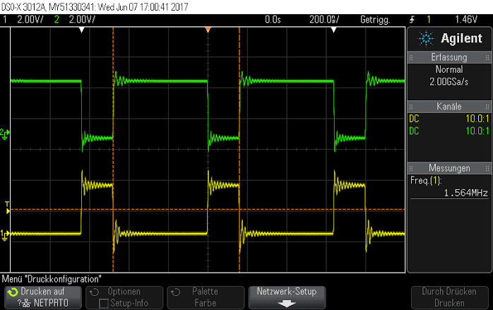
Tools Used
Recommended project tools:
- AMD Vivado
- ModelSim / QuestaSim
Hardware Details — Suitable FPGA Boards
Recommended FPGA implementation platform:
- Xilinx Zynq-7000 FPGA — selected for the project’s FPGA demonstration and implementation stage.
Why Choose Us?
Bangalore guidance for VLSI / FPGA / digital design students.
RTL & Testbench
Clean Verilog modules, self-checking testbenches and waveform documentation.
FPGA Bring-up
Constraint files, pin planning and on-board demo on Basys3 / Nexys / DE10.
Timing & Power
Synthesis reports, critical path notes and low-power coding guidelines.
Report & Viva
University-format documentation, PPT and expected viva questions.
FAQ
VLSI / FPGA Lab — Bangalore
RTL, simulation and FPGA implementation support.
Design
Waveforms
Synthesis
Demo
& Pin Map
Power Notes
IP Blocks
Support