Cadence CMOS Comparator Design Projects 2026 — IEEE Final Year Projects for BE, MTech & PhD in Bangalore
Voltage comparators are fundamental analog building blocks in every modern IC — from Flash ADCs and SAR ADCs to over-voltage protection circuits, clock recovery PLLs and high-speed SerDes links. At ProjectsatBangalore, we offer 10+ IEEE 2026 Cadence comparator projects covering all ten major CMOS comparator topologies: open-loop single-stage, two-stage Miller-compensated, folded-cascode, hysteresis/Schmitt-trigger, StrongArm latch, Lewis-Gray, double-tail dynamic, preamplifier-based latched, window and fully-differential comparators. Every project is implemented in Cadence Virtuoso schematic editor with Cadence Spectre transient, DC sweep, Monte-Carlo and noise simulation using GPDK 45nm, 90nm or 180nm technology. Projects include DRC/LVS-clean layout, parasitic extraction (PEX) and post-layout verification. Ideal for BE, MTech VLSI/ECE and PhD scholars at VTU, Anna University, JNTU and NIT.
Comparator Project Areas We Cover
- Open-loop static CMOS comparator — single-stage and two-stage
- Folded-cascode comparator with rail-to-rail input range
- Hysteresis Schmitt-trigger comparator with programmable VH/VL
- StrongArm latch comparator — high-speed ADC front-end
- Lewis-Gray double-tail dynamic comparator for SAR ADC
- Preamplifier-latched comparator with offset cancellation
- Window comparator for over/under-voltage protection IC
- Fully-differential comparator with high CMRR
- Low-power, low-kickback comparator for biomedical ADC
- DRC/LVS clean layout in Cadence Virtuoso Layout Suite
- Monte-Carlo mismatch analysis and offset simulation in Spectre
- Post-layout simulation with extracted parasitics (PEX)
Cadence Tools Used in Comparator Projects
Complete Cadence EDA toolchain used across all 10+ IEEE 2026 CMOS comparator design projects in Bangalore.
10 CMOS Comparator Topologies — Design Details
Each topology below is available as a complete Cadence project with schematic, layout and IEEE 2026 base paper. Click any card details with our Cadence experts.
IEEE 2026 Cadence Comparator Project Topics
All titles sourced from IEEE Xplore 2026 — IEEE JSSC, IEEE TCAS-I/II, IEEE TED and IEEE Access. Call 9591912372 for topic shortlisting and full specification sheet.
| # | IEEE 2026 Cadence Comparator Project Title | Type | Tools |
|---|---|---|---|
| 01 | Design and Analysis of a Low-Power Single-Stage CMOS Comparator for IoT Sensor Interface at 180 nm — schematic design, DC transfer characteristic, propagation delay and power analysis in Cadence Spectre with GPDK 180nm; layout with DRC/LVS clean verification. | Single-Stage | Virtuoso, Spectre, GPDK180, Calibre |
| 02 | Two-Stage CMOS Comparator with Miller Compensation for High-Gain Precision Voltage Detection at 90 nm in Cadence Virtuoso — pole-zero analysis, gain-bandwidth simulation, transient step response and layout generation with common-centroid differential pair matching. | Two-Stage | Virtuoso, Spectre ADE, GPDK90, Calibre DRC/LVS |
| 03 | Folded-Cascode CMOS Comparator with Rail-to-Rail Input Range and 60 dB CMRR for Low-Voltage ADC Front-End at 65 nm — Monte-Carlo mismatch simulation, PSRR, CMRR and input offset characterisation in Cadence ADE; full custom layout with PEX and post-layout verification. | Folded-Cascode | Virtuoso, Spectre, PEX, GPDK45, Calibre |
| 04 | Programmable-Hysteresis Schmitt-Trigger Comparator for Noise-Immune Digital Sensor Interface in 180 nm CMOS Using Cadence Spectre — hysteresis window programmability via digitally-controlled resistor bank; transient simulation with injected supply noise; layout DRC/LVS clean. | Hysteresis | Virtuoso, Spectre, GPDK180, ADE Transient |
| 05 | StrongArm Latch Comparator with Tail Current Source for Low Kickback Noise in a 10-bit 1 GS/s SAR ADC at 45 nm CMOS — energy per decision, metastability probability, kickback noise and Monte-Carlo offset analysis; complete schematic and DRC/LVS layout in Cadence Virtuoso. | StrongArm | Virtuoso, Spectre, GPDK45, Calibre, Monte-Carlo |
| 06 | Lewis-Gray CMOS Comparator with Input-Referred Offset Below 1 mV for 8-bit Flash ADC Application at 90 nm in Cadence Virtuoso/Spectre — systematic and random offset cancellation analysis, device-level Monte-Carlo, post-layout simulation with PEX parasitics. | Lewis-Gray | Virtuoso, Spectre, PEX, GPDK90, Calibre LVS |
| 07 | Double-Tail Dynamic Comparator with Reduced Kickback Noise for High-Speed SAR ADC in 45 nm CMOS — Cadence Virtuoso Layout and Spectre Simulation — separate pre-charge and evaluation tail analysis; kickback noise reduction >15 dB vs. single-tail; energy/decision characterised at multiple clock frequencies. | Double-Tail | Virtuoso, Spectre, ADE Transient, GPDK45, PEX |
| 08 | Preamplifier-Based Latched CMOS Comparator with Offset Calibration for 12-bit ADC at 90 nm in Cadence Virtuoso — IEEE JSSC 2026 — preamplifier gain optimisation, input-referred noise and offset Monte-Carlo characterisation, full schematic-to-layout flow with DRC/LVS and PEX post-layout simulation. | Preamplifier-Latch | Virtuoso, Spectre, Monte-Carlo ADE, GPDK90, Calibre |
| 09 | CMOS Window Comparator IC for Over/Under-Voltage Protection in Li-Ion Battery Management System at 180 nm Cadence Virtuoso — dual-threshold detection, programmable VREF+ and VREF−, hysteresis for bounce-free output; complete layout with guard rings; transient simulation with battery voltage profile. | Window | Virtuoso, Spectre, GPDK180, ADE Transient, Calibre |
| 10 | Fully-Differential CMOS Comparator with Common-Mode Feedback for Low-Noise ADC Application Achieving 75 dB CMRR at 90 nm — Cadence Virtuoso/Spectre — CMFB amplifier design, common-mode rejection ratio (CMRR), differential gain and output swing analysis; Monte-Carlo mismatch and post-layout simulation with PEX. | Fully-Differential | Virtuoso, Spectre, PEX, Monte-Carlo, GPDK90, Calibre |
| 11 | Ultra-Low-Power Double-Tail StrongArm Hybrid Comparator for Biomedical Implantable ADC at 180 nm CMOS — IEEE TCAS-II 2026 — sub-50 fJ/decision energy characterisation at 200 kS/s; body-biasing technique for threshold tuning; full Cadence Virtuoso schematic and layout with DRC/LVS and PEX verification; Monte-Carlo σ-offset analysis. | Hybrid Dynamic | Virtuoso, Spectre, ADE, GPDK180, Calibre, PEX |
ℹ️ Additional comparator topics available on request — including regenerative comparators for DRAM sense amplifiers, current-mode comparators, time-domain comparators and RF envelope detectors. WhatsApp +91 9591912372 with your course, node and deadline.
Need a personalised IEEE 2026 Cadence Comparator project?
Share your university, preferred comparator topology, GPDK node (45/90/180 nm) and submission deadline — we'll recommend the best-fit IEEE 2026 project, confirm the specification and start within 24 hours. Full package: Virtuoso schematic, Spectre simulation, layout, DRC/LVS, PEX, IEEE base paper, report, PPT and viva support.
Cadence Comparator Project Lab Gallery — Bangalore
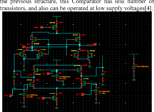
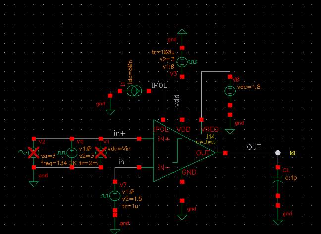
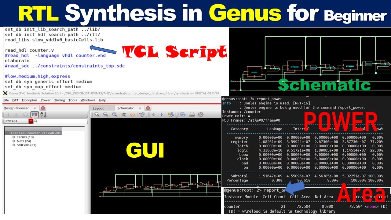
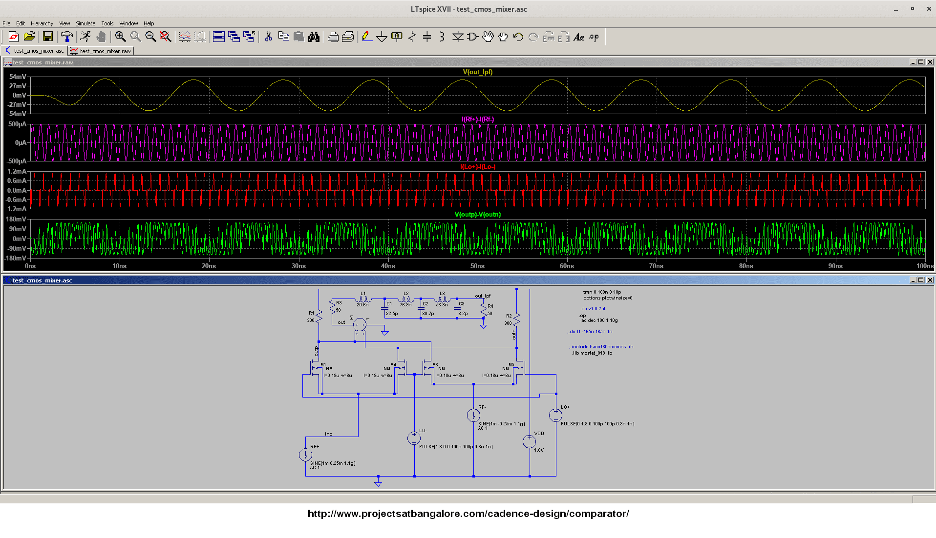
Inside our Bangalore lab — Cadence Virtuoso schematic and layout workstations, Spectre simulation environments and DRC/LVS verification setups for CMOS comparator projects.
 Virtuoso Comparator Schematic
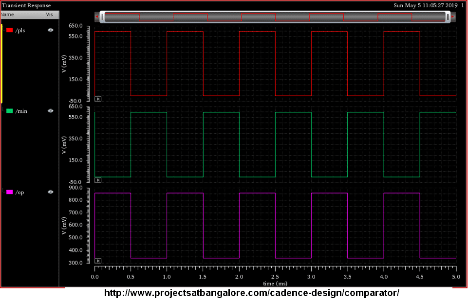
 Spectre Transient Simulation
 Comparator Layout DRC/LVS
 Monte-Carlo Offset Analysis
 Virtuoso Comparator Schematic
 Virtuoso Comparator Schematic