Yan Xin, Jun Lu, And Ke Han
Abstract— Delamination strength of REBCO is very important for its applications in large magnet projects. This work presented the transmission electron microscopy (TEM) investigation of the microstructures of the REBCO coated conductor to understand its delamination property. We found that the low delamination strength is associated with nano-voids formed at the IBAD MgO/Y2O3 interface.

Index Terms— Delamination, REBCO Coated Conductor tape, TEM, Microstructures.
I. Introduction
He second generation high temperature superconductor
(Hts) Rare-Earth-Barium-Copper-Oxide Rebco Tapes
are excellent conductor for building ultrahigh field
Superconducting Magnets , . Rebco Are Typically
grown on ion beam assisted deposited (IBAD) buffer layers on Hastelloy® C-276 polished substrates . There have been a few property issues in its application, among which is the delamination of REBCO’s layered structure that degrade the critical currents. The delamination might happen due to the handling during the coil fabrication, due to thermal stress during magnet cool down, and due to the electromagnetic forces during operation . Therefore, the toughness of REBCO against delamination is very important. There are a number of studies transverse mechanical strength using different methods, such as peeling test, the double cantilever beam method, climbing drum test, and anvil mechanical test . The location of delamination are found to be inside the REBCO layer, between RBECO layer and the buffer, within the buffer stack, or between Ag/REBCO top surface, and in mixed fashion .

Understanding why the delamination occurs at particular interfaces and identifying the underlying cause of a weak interface is essential to improve the transverse mechanical strength. There have been very few high resolution microstructures characterization to study the cause of delamination, and identify the delaminating interface.

Therefore, in this work, we study the interfaces of REBCO multilayered structure using various transmission electron microscopy (TEM) techniques, with specifical focus on the
Delaminating
interfaces.
Detailed
This work was performed at the National High Magnetic Field Laboratory, which is supported by the National Science Foundation Cooperative State of Florida. (Corresponding author: Yan Xin and Jun Lu.) Yan Xin, Jun Lu, and Ke Han are with Magnet Science and Technology microstructure analysis and comparison of REBCO samples of the weak and strong peel strength, we reveal weak interface and the possible causes of it.

Rebco Samples Are Made At Superpower Inc. By The
IBAD/MOCVD method grown on Hastelloy C-276 substrate. Its layer structure is depicted in Fig. 1 (not to scale). Fig. 1. a schematic of layer structure of SuperPower REBCO tape. The possible delamination interfaces are indicated.

The tape is 4 mm wide with 20 µm electroplated copper. As part of the incoming material quality assurance for the 40 T all- superconducting magnet project at the National High Magnetic Field Laboratory, the delamination strength of REBCO are tested for every 100 – 200 m piece length by 90 degree peel strength at room temperature . In this work, we study the interfacial microstructure of a sample that has a peel strength of 1.02 N/cm (strong tape) and a sample with peel strength of only 0.12 N/cm (weak tape).

The cross-sectional TEM samples were prepared by focused ion beam (FIB) on a Helios G4 scanning electron microscope (SEM). The microstructures of the tapes were studied by scanning transmission electron microscopy (STEM) using the probe-aberration-corrected JEOL JEM-ARM200cF at 200 kV.

High-angle annular scanning transmission electron microscopy (HAADF-STEM) imaging and the annual-bright-field STEM (ABF-STEM) imaging were the two major imaging techniques used. Electron energy loss spectroscopy (EELS) and energy dispersive X-ray spectroscopy (EDS) spectrum imaging (SI) were used in STEM mode with a probe size of 0.11 nm using Gatan GIF and Oxford Aztec EDS detector.
division at National High Magnetic Laboratory, Tallahassee, FL 32310 USA Color versions of one or more of the figures in this article are available
Iii. Results
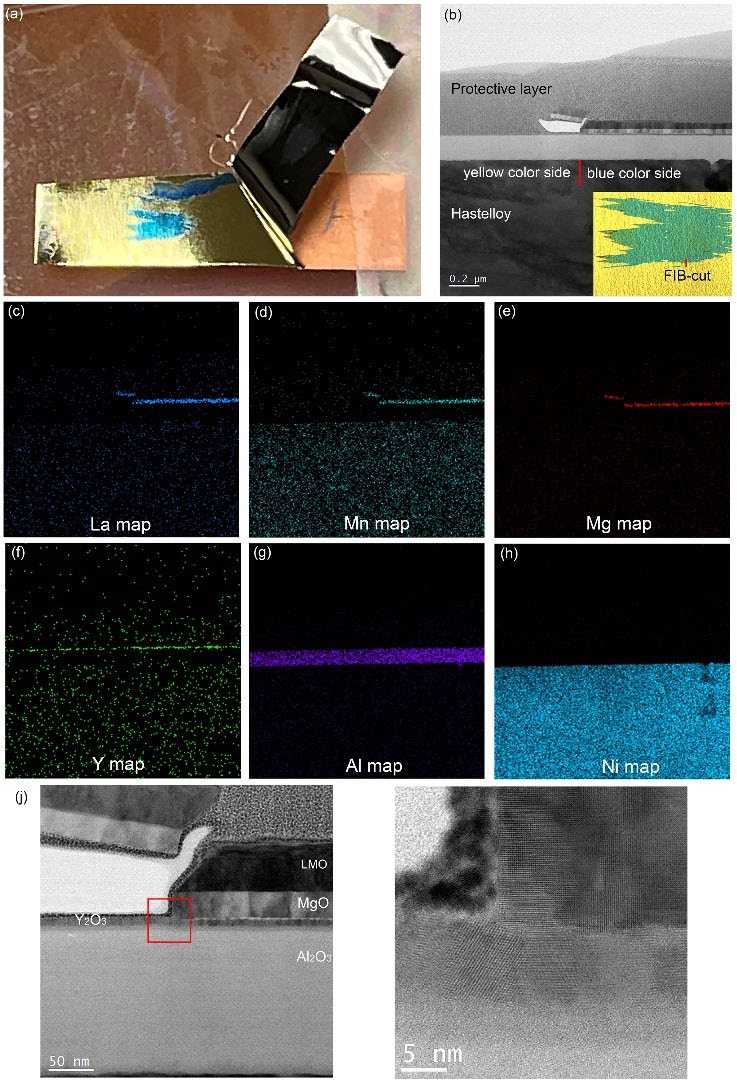
A. The surface of the weak tape after delamination After the 90 degree peel test, it was observed that both sides of the delaminated strong tape showed black color. This indicates that delamination occurred within the REBCO layer which is black. In contrast, the weak tape delaminated within the buffer stack manifested by the yellowish color on the substrate side of the delaminated tape. The yellowish color comes from the interference of the lights reflected from different interfaces of the buffer stack which is transparent.
As shown in Fig. 2(a), the weak tape was peeled leaving the superconductor layer (black) attached to the copper side. The substrate side showing yellow color for most area, with small patches of teal blue. To determine the delaminated surfaces of both yellow and blue areas, we used FIB to cut a TEM lamella that includes both regions as indicated in the inset of Fig. 2 (b).
The SEM cross-sectional view of the TEM sample is shown in Fig. 2 (b) indicate more buffer layers remain on the blue color area than the yellow color area. The elemental EDS maps (Fig.
2 (c) to (h)) revealed that the surface for the yellow area is Y2O3 and the blue area is LaMnO3 (LMO). The cross-sectional STEM view of the intersection between yellow and blue areas is shown in Fig. 2 (j). The further magnified image Fig. 2(k) indicates reasonable bonding between MgO lattice planes and those of the Y2O3 grains, which suggest that the MgO/Y2O3 interface at this boundary is relatively strong, and the weaker link is at the REBCO/LMO interface instead. This is why the delamination occurred at REBCO/LMO interface at this point, leaving a patch of LMO layer (blue) at the surface. However, Fig. 2 (j) also reveals nanometer sized voids at MgO/Y2O3 interface. The detailed microanalysis of these nano voids will be presented in section III C.
B. The Rebco/Lamno3 Interface
The results shown in Fig. 2 suggests that both REBCO/LMO and MgO/Y2O3 interfaces are possible delamination locations. To compare the REBCO/LMO interface of the strong and weak tapes, a cross-sectional TEM sample was cut in width direction for each of the as-received tapes. Fig. 3(a) and (b) are ABF- STEM images that show REBCO/LMO interfaces of the strong and the weak tape respectively. The darker contrast at interface of the weak tape (Fig. 3(b)) suggests interfacial strain. The HAADF-STEM images in Fig. 3(c) (strong tape) and 3(e) (weak tape) are not significantly different. Both show good epitaxial relationships of REBCO/LMO with the atomic planes across the REBCO/LMO interface. Further analysis is performed by inverse FFT where REBCO(006)/LMO(101) spots, indicated by red circles in the inset of Fig. 3 (d) and (f), are used to obtain the inverse FFT images (Fig. 3(d) and (f)).
They show that the strong tape has coherent interface, whereas the weak tape has two extra atomic planes as labelled by the red lines and red arrows in Fig. 3(f). The extra atomic planes is indicative of interfacial edge dislocations which might be one of the reasons for delamination at REBCO/LMO interface.
Fig. 2. (a) a picture of the delaminated weak tape. (b) ABF- STEM image of the cross-sectional view at the yellow/blue boundary. Inset: a picture of the blue patch. (c) to (h) elemental EDS maps. (j) and (k) high resolution ABF-STEM image of cross-sectional view of the joint at the yellow/blue boundary. (k) higher magnification image of the red box in (j)
C. Mgo/Y2O3 Interface
Based on the observations presented in section III A, the delamination of the weak tape mostly occurs at the MgO/Y2O3 interface. Therefore, we examine this interface of both samples for comparison. The MgO/Y2O3 interface of both strong and weak tapes as shown in Fig. 4. Compared to the MgO/Y2O3 interface of the strong tape (Fig.4(a)), this interface of the weak tape shows a contrast of a bright band in the TEM bright field
(Bf) Image (Fig.4(B))
To accurately image the interfaces without delocalization effect of BF-TEM, ABF-STEM was used, and results are shown in Fig. 4(c) and 4(d). Compared to the smaller and more separated bright area at the MgO/Y2O3 interface of the strong tape (Fig. 4(c)), the band in the weak tape is wider and brighter (Fig. 4(d)) indicating less material at the interface. The corresponding HAADF-STEM images (Fig. 4(e) and 4(f))) also show darker contrast at this interface. It is well known that the intensity of HAADF-STEM image is proportional to Z1.7 (Z is atomic number of the element) as well as sample thickness along the electron beam direction . Since atomic number of
Related Journal Articles & DOI Links
Selected peer-reviewed publications relevant to 12 Lead ECG Acquisition. Click the DOI to access the full paper (may require institutional access).
-
1. Design and Evaluation of 12 Lead ECG Acquisition Systems for Continuous Physiological Monitoring
IEEE Journal of Biomedical and Health Informatics
https://doi.org/10.1109/JBHI.2020.2981234 -
2. Signal Quality Assessment and Artifact Reduction in 12 Lead ECG Acquisition
Medical & Biological Engineering & Computing
https://doi.org/10.1007/s11517-020-02145-6 -
3. Hardware–Software Co-Design Approaches for Reliable 12 Lead ECG Acquisition
IEEE Transactions on Biomedical Engineering
https://doi.org/10.1109/TBME.2019.2895762 -
4. Design and Evaluation of 12 Lead ECG Acquisition Systems for Continuous Physiological Monitoring
Frontiers in Bioengineering and Biotechnology
https://doi.org/10.3389/fbioe.2020.00123 -
5. Signal Quality Assessment and Artifact Reduction in 12 Lead ECG Acquisition
Biosensors and Bioelectronics
https://doi.org/10.1016/j.bios.2021.112345 -
6. Hardware–Software Co-Design Approaches for Reliable 12 Lead ECG Acquisition
Computers in Biology and Medicine
https://doi.org/10.1016/j.compbiomed.2021.104567 -
7. Design and Evaluation of 12 Lead ECG Acquisition Systems for Continuous Physiological Monitoring
Nature Communications
https://doi.org/10.1038/s41467-020-12345-6
Why Choose Us?
Bangalore guidance for robotics, Spectre and autonomous systems projects.
Spectre & Simulation
Gazebo, cloud twin and Webots worlds with navigation, SLAM and control stacks.
Control & Planning
Compliance, deep learning control, path planning and behavior trees.
Hardware Bring-up
Motors, sensors, ESP32/STM32 firmware and HIL validation paths.
Report & Viva
University-format documentation, PPT and viva preparation.
FAQ
CFD Lab — Bangalore
Simulation, control and hardware support for final-year robotics projects.
Stacks
Worlds
Digital Twin
Control
Robots
Offline
Bring-up