1088
Chip-Scale Coils for Millimeter-Sized Bio-Implants
Maysam Ghovanloo
Abstract—Next generation implantable neural interfaces are targeting devices with mm-scale form factors that are freely floating and completely wireless. Scalability to more recording (or stim- ulation) channels will be achieved through distributing multiple devices, instead of the current approach that uses a single cen- tralized implant wired to individual electrodes or arrays. In this way, challenges associated with tethers, micromotion, and relia- bility of wiring is mitigated. This concept is now being applied to both central and peripheral nervous system interfaces. One key re- quirement, however, is to maximize specific absorption rate (SAR) constrained achievable wireless power transfer efficiency (PTE) of these inductive links with mm-sized receivers. Chip-scale coil struc- tures for microsystem integration that can provide efficient near- field coupling are investigated. We develop near-optimal geometries for three specific coil structures: in-CMOS, above-CMOS (planar coil post-fabricated on a substrate), and around-CMOS (helical wirewound coil around substrate). We develop analytical and sim- ulation models that have been validated in air and biological tissues by fabrications and experimental measurements. Specifically, we prototype structures that are constrained to a 4 mm× 4 mm silicon substrate, i.e., the planar in-/above-CMOS coils have outer diam- eters <4 mm, whereas the around-CMOS coil has an inner diam- eter of 4 mm. The in-CMOS and above-CMOS coils have metal film thicknesses of 3-µm aluminium and 25-µm gold, respectively, whereas the around-CMOS coil is fabricated by winding a 25-µm gold bonding wire around the substrate. The measured quality fac- CMOS). Also, PTE of 2-coil links based on three types of chip-scale coils is measured in air and tissue environment to demonstrate tissue loss for bio-implants. The SAR-constrained maximum PTE measured (together with resonant frequencies, in tissue) are 1.64% Index Terms—Chip-scale coil, implantable neural microsystem, integrated coil, mm-sized coil, microfabricated coil, near-field cou- pling, wirewound coil, wireless power transmission.
Manuscript received March 9, 2018; revised May 12, 2018 and June 22, 2018; accepted June 28, 2018. Date of publication July 20, 2018; date of current version October 19, 2018. This work was supported in part by the Engineering and Physical Sciences Research Council (EPSRC) Award EP/M020975/1, and in part by the National Science Foundation (NSF) Awards ECCS-1408318 and ECCS-1407880. This paper was recommended by Associate Editor Prof. Sandro Carrara. (P. Feng and P. Yeon contributed equally to this work.) (Corresponding
Author: Peilong Feng.)
P. Feng and T. G. Constandinou are with the Centre for Bio-Inspired Tech- London, South Kensington Campus, London SW7 2AZ, U.K. (e-mail:,peilong. P. Yeon and M. Ghovanloo are with the GT-Bionics Laboratory, School of Electrical & Computer Engineering, Georgia Institute of Technology, Atlanta, Y. Cheng is with the School of Electronic & Information, Hangzhou Dianzi Color versions of one or more of the figures in this paper are available online Digital Object Identifier 10.1109/TBCAS.2018.2853670
M
ILLIONS of people worldwide are affected by neurolog- ical and psychiatric disorders, in addition to damages to the nervous system due to stroke, spinal cord injury (SCI), or traumatic brain injury (TBI). Emerging technologies that pro- vide the capability of direct neural interfacing offer the prospect of new therapies and treatments. Even at present, most human trials in Brain Machine Interfacing (BMIs) are utilizing percu- taneous wired connections for powering and communication.
Breaking through the skin (or tissue), however, poses a sig- nificant risk of infection . A tethered approach additionally requires anchoring a rigid micro-electrode array (MEA) within soft, delicate tissue. Therefore, the associated micro-motion in- creases the risk of damage to the blood-brain barrier (BBB) that can lead to scar formation and failure of the device in the long run . It is thus highly desirable to have devices that can avoid the tethering problem by utilizing Wireless Power Transfer (WPT) .
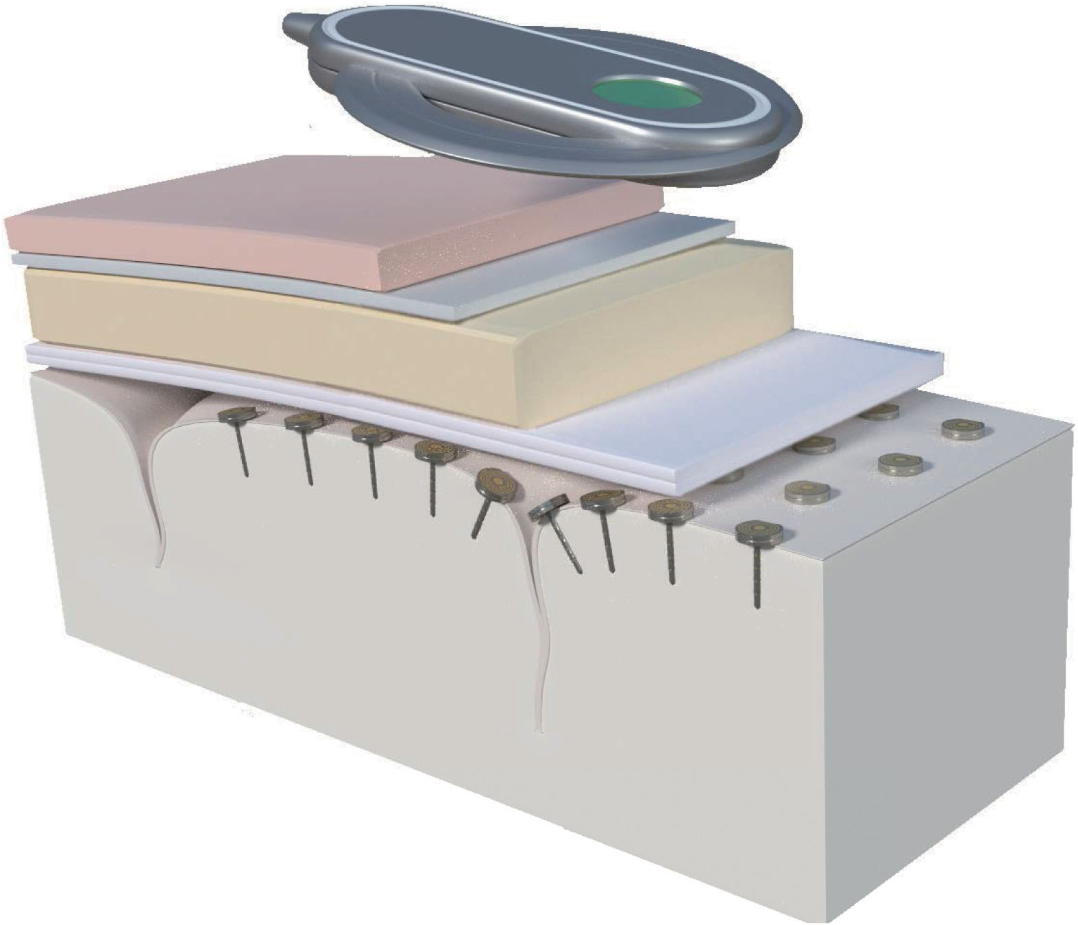
Over the past few years, there have been new efforts in devel- oping wireless, free-floating microsystems that achieve scala- bility through a distributed approach, i.e. using multiple devices that are sub-mm or mm-scale. These devices are being devel- oped for both the peripheral and central nervous systems, such as electroceuticals, and BMIs, respectively –. This concept is illustrated in Fig. 1, for a subdural BMI, utilizing near-field coupling for WPT.
Several methods have been proposed to power these sub-mm and mm-scale neural implants, including: ultrasonic , ,
Midfield , And Near-Field Powering , –. Ultra-
sound maintains efficient energy transmission for subcutaneous implants when they are perfectly aligned, but it is not suitable for powering distributed or intracranial implants due to its sig- nificant attenuation through the skull and extreme sensitivity on depth and orientation misalignments of the piezo-crystals. Mid- field energy transmission results in significantly less allowable power delivered to the load (PDL) because of the higher spe- cific absorption rate (SAR) in tissue at high frequencies instead, despite its ability in focusing the electromagnetic (EM) field on the location of the implant. Near-field WPT, on the other hand,
Has A Few Advantages As Follow:
Firstly, the maximum allowable PDL is larger than that of the mid-field because of the lower SAR in the tissue at lower frequencies , . Secondly, near-field WPT experiences negligible channel variations in tissue, as opposed to mid-field transmission, in which propagation delays dominate because of the inhomogeneous permeability of tissue at higher frequencies , . Therefore, near-field WPT seems to be more suitable This work is licensed under a Creative Commons Attribution 3.0 License. For more information, see http://creativecommons.org/licenses/by/3.0/ FENG et al.: CHIP-SCALE COILS FOR MILLIMETER-SIZED BIO-IMPLANTS
1089
Fig. 1. Concept of a distributed implantable BMI with freely-floating neural probes that use mm-scale secondary coils for wireless powering.
and reliable for powering the mm-scale implants through the lossy biological medium. The power transfer efficiency (PTE) of inductive links to power mm-scale implants are often very low (a few percents) due to their relatively large coil separation, and arbitrary loca- tions and orientations of implants . There have been efforts to improve the SAR-constrained PTE for mm-scale devices and provide meaningful levels of PDL (0.1–1 mW) by optimizing the inductive link geometry , , . Much of the work reported to date, including , focus on a single method wire- wound coils (WWCs), and as such, do not explain the pros and cons of utilizing alternative technologies. For instance, there has already been much work in integrated coils for RFIC designs such as , , . However, the quality factor (Q) of inte- grated coils remains limited (<10). This is because the CMOS technologies can only support metal layers that are relatively thin (1–4 μm), and suffers from losses due to eddy currents, par- ticularly when the substrate resistivity is low . Even using advanced techniques, such as multiple metal layers connected in parallel using vias , or patterned ground shields , result in modest gains. There have also been a number of CMOS- compatible MEMS technologies proposed to improve Q, such as developing suspended coils above the substrate , , or utilization of polymer enhanced through-silicon-vias .
We present different methods of developing mm-scale coils for integration with CMOS microelectronics for distributed im- plantable neural microsystems. We refer to them in the rest of this paper as in-CMOS (fully-integrated coils), above-CMOS (post-processed on top of CMOS substrate), and around-CMOS (wirewound around the CMOS chip). This study builds upon our earlier work , now extended to three types of coils by adding above-CMOS coils into our comparison. Also, around- CMOS coil has comparable dimensions (4 mm × 4 mm) to the above-CMOS and in-CMOS coils (previously this was 1 mm × 1 mm). Furthermore, we have derived analytical models, op- timize design through computational methods, fabricated the coils, and compared their performance through measurements of the individual coils but also the 2-coil link in both air and tissue. Section II introduces analytical models for the different Fig. 2.
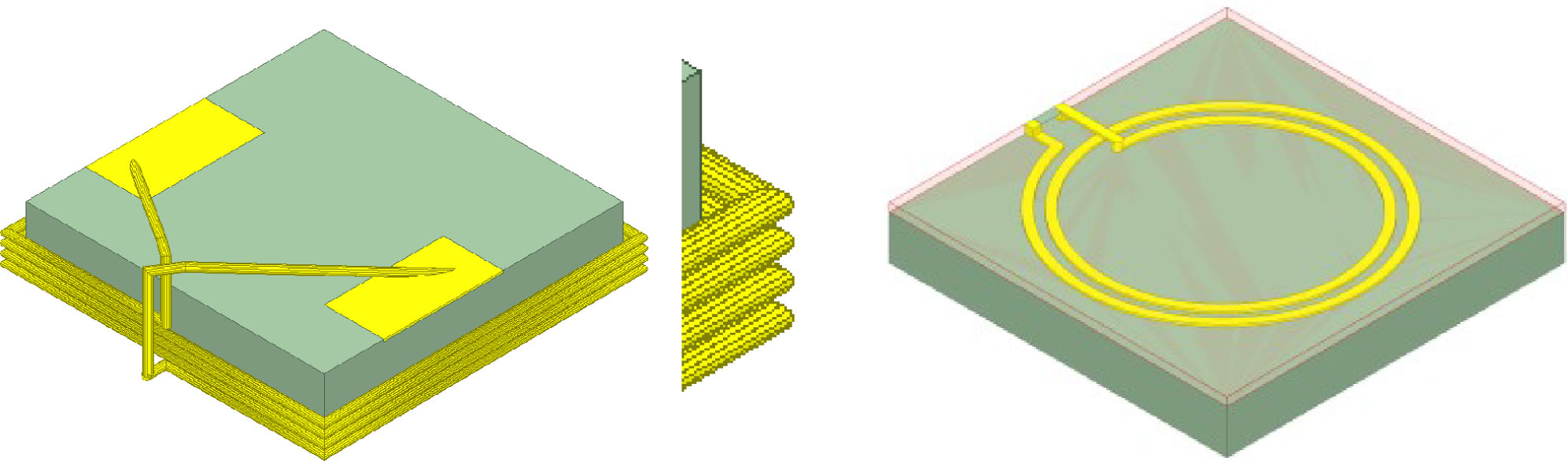
3D illustration for (a) around-CMOS (i.e. wirewound) coil; and (b) on- CMOS and above-CMOS (i.e. on substrate) coils, and equivalent circuit models for (c) around-CMOS coil and (d) on-CMOS and above-CMOS coils.
coil types. Section III describes the fabrication process for each coil type and optimization paradigm using simulation models to maximize the PTE. Section IV presents measurement re- sults, while also exploring practical matters, such as electromag- netic properties, manufacturability, reliability and performance modification made by the presence of the tissue environment.
Section V discusses the potential impact of integration with the rest of the implant, particularly the packaging on the coil per- formance, and the effects of surrounding tissue environment, followed by conclusions.
Ii. Analytical Coil Model
This section presents analytical models for three different types of coils; in-CMOS, above-CMOS and around-CMOS, for powering mm-sized implants. Key geometric parameters of the around-CMOS coil are illustrated in Fig. 2(a), where Do2 is the coil side length, rw2 is the wire radius, p2 is the center-to- center pitch between adjacent turns, and l2 is the solenoid length.
Fig. 2(b) illustrates 3D model of a planar spiral coil, which is valid for both in-CMOS and above-CMOS types with key ge- ometrical parameters: Do2 the outer diameter, Di2 the inner diameter, w2 the trace width, and s2 the spacing between adja- cent traces. N2 is the number of turns for all types of coils on the power receiving side. The equivalent circuit model with lumped RLC elements for around-CMOS and both in-CMOS and above- CMOS (substrate-based) coils are shown in Figs. 2(c) and 2(d) , respectively, where Ls2 and Rs2 are the series-connected induc- tance and parasitic resistance, and Cp2 and Rp2 are the parallel- connected parasitic capacitance and resistance, respectively. The parasitics elements associated with the substrate can be modeled by three components: Rsi2 the substrate resistance determined by majority carrier concentration, Csi2 the substrate capacitance associated with high dielectric silicon media, and Cox2 the sili- con oxide capacitance . The eddy current through the silicon
1090
substrate can be estimated using resistance Re2, inductance Le2, and capacitance Ce2. The geometry-dependent expressions that estimate the coils’ self-resonance frequency (SRF) of mm-scale coils based on the lumped RLC elements in Figs. 2(c) and 2(d) are presented in the following subsections.
A. Around-Cmos (Wirewound) Coil Model
Equivalent circuit model for around-CMOS coil is relatively simple because the silicon substrate does not significantly af- fect the electrical properties of this type of coil because of the sufficient spacing between the silicon substrate and coil conduc- tors. The serial inductance Ls2 of the around-CMOS coil can be
(3)
where effective magnetic permeability Uef f is determined by the relative permeability of surrounding materials. KL is a cor- rection factor for the assumption of having a uniform magnetic field across the solenoid, and KP models the effect of large pitch.
rH F is the effective wire radius considering the skin effect at operating frequency, and can be found from , equation (4) shown at the bottom of this page, where Rs2 represents the sum of skin effect resistance, Rsk, and proximity effect resistance,
(8)
where ρ is the metal resistivity, and Hn is the magnetic fields under the net current flowing through the solenoid coil I0, μr is the relative permeability of the conductor. ber(m) and bei(m) are Kelvin functions .
Cp2 and Rp2 can be precisely modeled using equivalent lumped elements in series or parallel connection with coeffi- cients for fitted curve polynomials estimated using COMSOL (Los Angeles, CA) simulation. Their equations and table con- taining the curve-fitting coefficients are described in .
B. In-CMOS and Above-CMOS (substrate-based) Coil Model These coil types are based on planar spiral coils conduc- tive substrate and thus have somewhat more complex analytical model, as shown in Fig. 2(d). The spiral inductance is estimated by using current sheet approximation .
(10)
Values for c1 to c4 can be found from , which only relate to the shapes of the planar spiral coils. N2 is the number of turns and φ is the filling factor. Similar to around-CMOS coil, parasitic series resistance Rs2 consists of Rsk and Rpr. Rpr is expressed in equation (7) and Rsk can be written as:
(13)
where t2, w2 and l2 are the thickness, width and length of con- ductor tracks, respectively. Similar to the around-CMOS coil model, the parallel parasitic capacitance Cp2 and the paral- lel parasitic resistance Rp2 are caused by the dielectric loss of the coating materials and the biological tissues. In addi- tion, this equivalent model contains the substrate capacitance Csi2, substrate resistance Rsi2, and silicon oxide capacitance Cox2 .
(16)
where CSub and GSub represent the unit capacitance and con- ductance of silicon substrate. tox2 and εox2 are the thickness and permittivity of silicon dioxide. The current in the coil generates eddy currents on the silicon substrate that are not negligible and cause a parasitic inductance Le2 and resistance Re2 –,
1.3(W2 + S2)0.93L2
−1.4.
(18)
rH F = 0.5Do2(1 −(2rw2/Do2)2)(p2/2rw2 −1) + Do2 −2rw2 + 2rw2/N2
(4)
FENG et al.: CHIP-SCALE COILS FOR MILLIMETER-SIZED BIO-IMPLANTS
1091
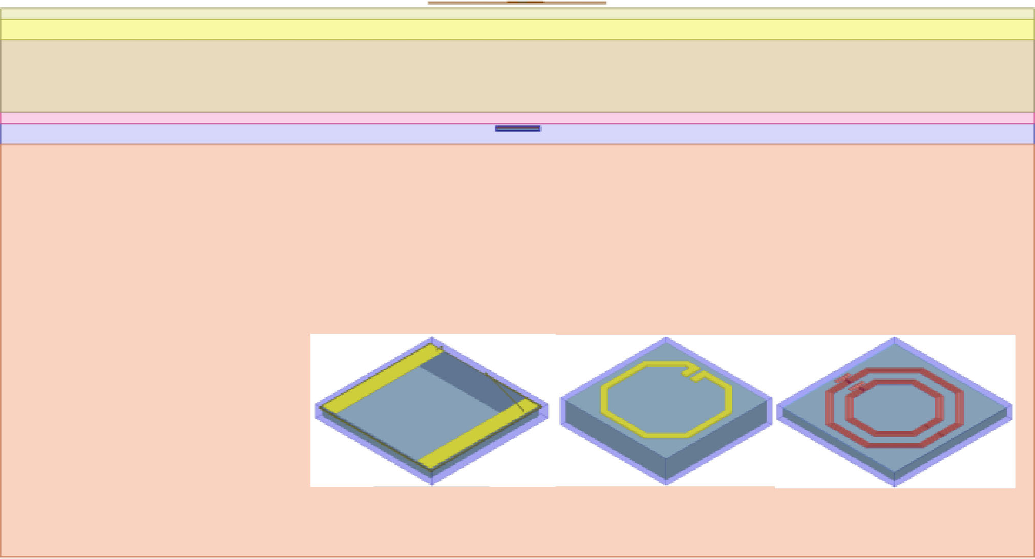
Fig. 3. Cross-section of the human head model and relative positions of the Tx and Rx coils. Inset: Rx coil models (a) around-CMOS (wirewound coil, WWC); (b) above-CMOS (microfabricated MEMS); (c) in-CMOS coils.
A. Simulation Setup
The electromagnetic (EM) simulation model of the inductive link is setup in HFSS (ANSYS, Canonsburg, PA) environment, which is a 3D full-wave EM field solver based on finite element analysis (FEA). Fig. 3 shows the cross-section of the EM sim- ulation model of the mm-scale Rx coil, L2, around a 10 cm× 10 cm × 5 cm human head model with a transmitter (Tx) coil, L1, placed above it. The frequency-dependent dielectric prop- erties of skin, subcutis (fat), skull (bone), cerebrospinal fluid (CSF), dura, and brain are fed into this EM simulation model based on . The nominal distance between L1 and L2 is con- sidered to be d12 = 12 mm, which is the nominal scalp-to-cortex distance . The air-gap between L1 and the skin is often a ge- ometrical parameter to be optimized, but we have also fixed it to be 0.6 mm since d12 is fixed at 12 mm for fair PTE comparison among three types of coils. L2 is placed in the CSF and covered with 100 μm of polydimethylsiloxane (PDMS). The center of L2 is aligned with the center of L1. These 2-coil inductive links aim to deliver 111 μW to 9 kΩ load resistance at 1 Vrms across the secondary LC tank. To allow for a fair comparison between these three coil types, the size of the silicon substrates is chosen to be 4 mm × 4 mm based on the estimates of the area needed for the implantable device integrated electronics.
Tx coils for three types of Rx Coils are individually optimized in air and tissue models to maximize the PTE of the 2-coil links in two different surrounding environment. Since Tx coils are located outside the body, this eases the size and material limi- tations, making it possible to use higher electrical conductivity copper (5.96 × 10⁷ S/m) to design cm-scale Tx coils instead of gold (4.10 × 10⁷ S/m) or aluminum (3.77 × 10⁷ S/m) for Rx coils. Detailed specifications of the Tx coils are listed in Table I.
The three different Rx coil structures are shown in the inset in Fig. 3: around-CMOS (with insulated bond-wire); above-CMOS (post fabricated); and in-CMOS coils. For the around-CMOS coil, an insulated Au bond wire with 25 μm diameter, 2rw, is wound around the substrate, with its terminals bonded to a pair of pads on the surface of silicon substrate. The above-CMOS coil is electroplated with a 25 μm thick Au layer on the silicon substrate. The in-CMOS coil is designed in HFSS and imported
Optimal Geometries And Electrical Properties Of Rx Coils
to the Virtuoso Layout Suite (Cadence Design Systems Inc., San Jose, CA). The fabrication process for the CMOS coil is AMS 0.35 μm 4M, 2P, 50 V technology (H35B4S1, ams AG, Austria). In this process, metal layers 1–3 are 640 nm, and top metal layer is 3 μm thick. The in-CMOS coil uses MET3 and MET4 layers connected in parallel (using VIA3) to increase the total metal trace thickness to 4 μm (considering the thickness of VIA3). Slots are added to metal traces to meet the design rules and relieve the surface tension of the metal layers.
B. Optimization
Fig. 4(a) shows the equivalent circuit model of 2-coil in- ductive link for powering mm-scale implants. For impedance matching at a target resonant frequency f0, a tuning capacitor C2 often connected with Ls2 in parallel or series, depending on the value of the original load resistance RL,O. In most cases for powering mm-scale implants, RL,O is in the order of kΩ, and a parallel C2 is preferable since it results in a larger loaded Q factor, Q2L , . Fig. 4(b) shows the simplified equivalent circuit for all coils. The right side of Fig. 4(b) is a simpli- fied equivalent circuit of both Figs. 2(c) and 2(d) when one side of the inductor is connected to ground and placed in se-
S2/(Rl,O||Rp2). For A Large Load
RL << |1/(jwCox2) + Rsi2||1/(jwCsi2)|, the loss by the sil- icon substrate can be ignored. However, for most implantable applications, the loss through the silicon substrate cannot be negligible since RL ≈|1/(jwCox2) + Rsi2||1/(jwCsi2)|. To minimize the substrate loss for the above-CMOS coil, several
1092
Fig. 4. Equivalent circuit models for: (a) 2-coil inductive link for powering mm-scale Rx coil; (b) mm-scale Rx coil with a silicon substrate.
techniques exist such as physically decoupling the coil from the lossy silicon substrate , or replacing the silicon
Substrate With Polymer . As Described In , , ,
because of the very small coupling, ≤0.01, between Ls1 and Ls2, the geometric design and optimization of the Tx and Rx coils can be completed independently. Therefore, the PTE can
(19)
where Tx figure of merit (FoM), TxF oM , represents the cou- pling strength between Tx and Rx coils. Rx power reception susceptibility, RxP RS, indicates how much power can be re- ceived and passed to RL . k12 is the Tx-Rx coils’ coupling coefficient. Q1 and Q2L are the Q factors of the Tx and loaded Rx coils. ηRx is the ratio of the power delivered to RL to the power dissipated in the secondary coil due to its parasitic resis- tance, Rs2.
1) Optimizing Rx: After applying the common design con- straints such as Do2 = 4 mm, each coil was designed by follow- ing the coil optimization procedure in , , in a way to maximize RxP RS, which is a multiplication between the loaded Q factor, Q2L = wLs2/(Rs2 + RL), and the Rx inter- nal efficiency, ηRX = RL/(R2 + RL)). For the around-CMOS design, p2 is fixed because this design parameter is not control- lable during the semi-manual coil fabrication. Considering the diameter of the commercially available insulated bonding-wire, 2rw is chosen to be 25 μm. N2 was swept in the HFSS model and MATLAB (MathWorks, Natick, MA) using the analytical model presented in Section II. For the design of in-CMOS coil, the thickness and material of metal layers are defined by the CMOS process, consequently, its Q2 is mainly limited by se- ries resistance RS2 . The geometric optimization for the in-CMOS coil thus focuses on the number of turns N2 and Fig. 5.
Simulated SAR in head model at optimal frequencies for in-CMOS, around-CMOS and above-CMOS coils with fixed 10 mW Tx power. width-to-spacing ratio w2/p2 . Gold (Au) is selected for above-CMOS coil for its high conductivity and biocompatibil- ity. In addition, the thickness of the metal traces is not limited by the CMOS process, and can be optimized in HFSS and fab- ricated up to a certain limit by electrochemical deposition to reduce RS2.
The optimal geometry of the Rx coil in the tissue medium often tends to have fewer turns and a smaller trace width than the one in air. This means that the coil has a smaller contact surface with the lossy tissue medium. The geometric dimensions of three Rx coils have thus been individually optimized in the human head model for IMDs. They have then been simulated in the air environment to reveal alterations of EM properties with the presence of biological tissues. The geometries and electrical properties of these coils after optimizations are shown in Table I.
2) Maximizing PTE: Since the PTE is a multiplication of TxF oM and RxP RS, the Tx geometry to maximize the PTE is explored in this subsection. PTE is largely dependent upon
(20)
where Do1 is the outer diameter of the Tx coil. (20) implies that k12 is dependent mostly on Do1 considering that Do2 is a Rx design constraint and d12 is fixed at 12 mm for this study.
Therefore, the optimal Do2 was found first to maximize k12 and rest of Tx parameters were found to achieve the maxi- mum TxF oM . The geometrical and electrical parameters of the 2-coil inductive link for three different Rx coils are summarized in Table I.
The operating frequency of each inductive link is individu- ally optimized by adopting the methodology in , , . According to optimized simulation results in Table I, around- CMOS, above-CMOS and in-CMOS coils in biological tissue environments operate at 300 MHz, 330 MH and 60 MHz, re- spectively. To ensure the human exposure to electromagnetic radiation at these frequencies within the safe levels, the SAR of these 2-coil links have been simulated with the fixed 10 mW transmitting energy and reported in Fig. 5. The operating fre- quency of the above-CMOS coil is relatively low compared to FENG et al.: CHIP-SCALE COILS FOR MILLIMETER-SIZED BIO-IMPLANTS
1093
Fig. 6. Process steps of the above-CMOS (micro-fabricated) coil. the others, so its SAR dramatically drops to 3.57E-3 W/Kg. The rest of the two Rx coils operate at higher frequencies and their standard of 1.6 W/Kg .
C. Fabrication
Implementation of the above-CMOS (micro-fabricated) coil requires mainly photolithography and electroplating processes. Fabrication procedure of the on-CMOS coil is shown in Fig. 6. A 50 nm chromium (Cr) adhesive layer and 100 nm Au seed layer are deposited on a 4-inch silicon wafer using electron-beam physical vapor deposition (PVD). Subsequently, the AZ4562 photoresist (Microchemicals GmbH, Germany) is spin coated twice on the wafer at 1400 rpm for 40 s to reach 25 μm thickness.
The profiles of coils are exposed and developed on photoresist layer by Dilase 250 photolithography system (Kloe, France). Then, 25.1 μm Au layer is added by electrochemical deposition.
Following 183 min electroplating, the remaining photoresist and global thin Au/Cr layers are removed. The around-CMOS coil is fabricated by winding a 25 μm insulated bondwire (Microbonds, Canada) around the 4 mm × 4 mm passive silicon die with a manual wire-bonder (Westbond 7476D, Anaheim, CA) and a stepper motor. The silicon die was fixed in the center of a QFN package. One terminal of the bonding-wire is ultrasonically bonded on the QFN package, which is placed on top of the stepper motor. The silicon die is then slowly rotated by the stepper motor, and position of the wedge is carefully adjusted in a way that the bonding wire is wound around the silicon die. Once the motor is revolved up to the target number of turns, the other end of bonding-wire is ultrasonically bonded on the QFN package. Afterwards, instant glue is applied to the four corners of the die to fix the coil in place. In an actual implant, two ends of bonding-wire will be attached directly on the active CMOS chip. In this case, however, they are lifted along with the passive silicon die and attached to designated pads on a PCB for measurements.
Details of the fabrication procedure can be found in . As described in Section II, the in-CMOS coil is fabricated in AMS 0.35 μm CMOS technology featuring a 3 μm thick top metal layer, and the top two metal layers are connected using VIA3 to create a 4 μm thick metal trace. The 10 μm slots are added to the metal trace to extend the effective width of the metal trace to 175 μm. Two terminals of the coils are connected to the 100 μm × 100 μm pads, which are arranged for ground- signal-ground-signal-ground (GSGSG) of RF probes.
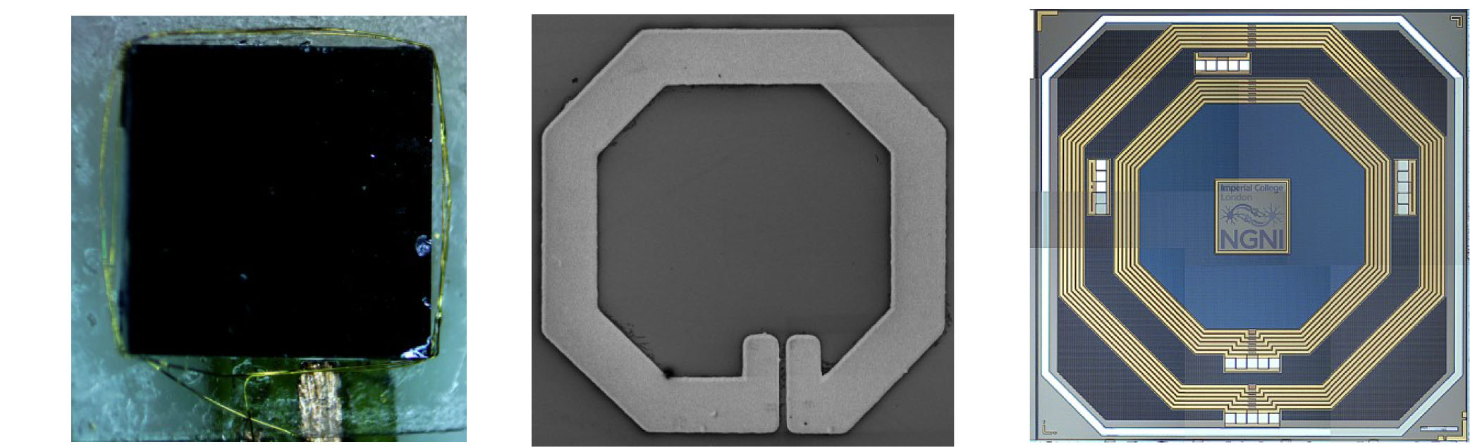
The abovementioned coils are shown in Fig. 7. The inner octagonal shape coil in Fig. 7(c) is not relevant to this Rx coil comparison study.
Fig. 7. Fabricated (a) around-CMOS; (b) above-CMOS; and (c) in-CMOS coils.
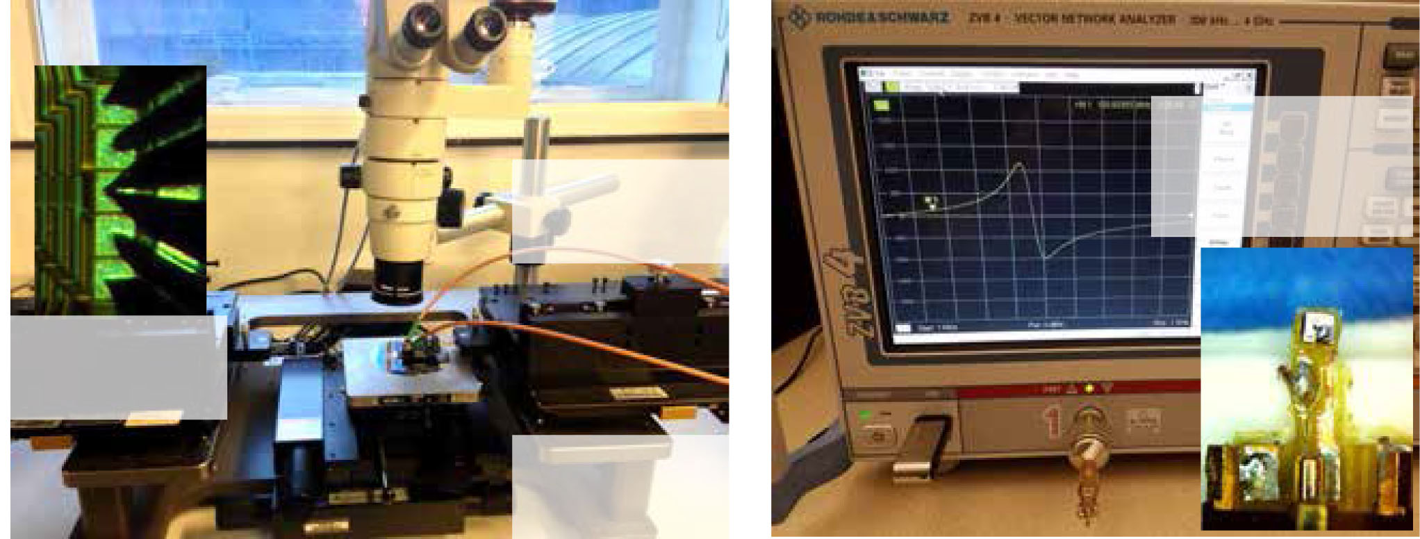
Fig. 8. In air measurement setups for: (a) the planar (in-CMOS and above- CMOS) coils; and (b) the wirewould (around-CMOS) coil.
A. Measurement Setup
1) In Air Measurement Setup: The planar (in-CMOS and above-CMOS) coils are measured using E8361A network ana- lyzer (Agilent, CA), Model 40A probe (Picoprobe, FL, USA), ACP350 probe (Cascade Microtech, Oregon, USA) and probe station (Cascade Summit 9101, OR, USA). The measurement setup is shown in Fig. 8(a). To calibrate the network analyzer, the fabricated patterns for short-open-load (SOL) are utilized to eliminate parasitics from the cable and probes.
The around-CMOS coil is measured using a ZVB4 vector net- work analyzer (Rohde & Schwarz, Germany) in Fig. 8(b) mea- surement setup. The coil terminals are bonded to two pads on a T-shaped PCB that is connected to an SMA connector. To reduce the parasitic effects, measurements were calibrated using the de- embedding method. It involves subtracting the Y-parameters of the open-circuited PCB to remove the parasitic capacitance and resistance in parallel and subtracting the Z-parameters of the short-circuited PCB to remove the series parasitic inductance and resistance .
2) Ex vivo measurement setup: Fig. 9 shows the experimen- tal setup for ex vivo measurements. The fresh 11 mm lamb ribs are inserted between the Tx and Rx coils. The Rx coils connect to a 2 cm × 5 cm PCB with an SMA connector via bonding wires, and the Tx coils are fabricated by utilizing 1 oz copper PCB and 2 oz copper foil. Both coils are tuned to the optimal operating frequency by using tuning capacitors, according to the simulation results in Table I. In addition, the impedance match- ing networks guarantee that the energy can be injected into the 2-coil inductive links from the VNA standard 50 Ω ports.
Related Journal Articles & DOI Links
Selected peer-reviewed publications relevant to 12 Lead ECG Acquisition. Click the DOI to access the full paper (may require institutional access).
-
1. Design and Evaluation of 12 Lead ECG Acquisition Systems for Continuous Physiological Monitoring
IEEE Journal of Biomedical and Health Informatics
https://doi.org/10.1109/JBHI.2020.2981234 -
2. Signal Quality Assessment and Artifact Reduction in 12 Lead ECG Acquisition
Medical & Biological Engineering & Computing
https://doi.org/10.1007/s11517-020-02145-6 -
3. Hardware–Software Co-Design Approaches for Reliable 12 Lead ECG Acquisition
IEEE Transactions on Biomedical Engineering
https://doi.org/10.1109/TBME.2019.2895762 -
4. Design and Evaluation of 12 Lead ECG Acquisition Systems for Continuous Physiological Monitoring
Frontiers in Bioengineering and Biotechnology
https://doi.org/10.3389/fbioe.2020.00123 -
5. Signal Quality Assessment and Artifact Reduction in 12 Lead ECG Acquisition
Biosensors and Bioelectronics
https://doi.org/10.1016/j.bios.2021.112345 -
6. Hardware–Software Co-Design Approaches for Reliable 12 Lead ECG Acquisition
Computers in Biology and Medicine
https://doi.org/10.1016/j.compbiomed.2021.104567 -
7. Design and Evaluation of 12 Lead ECG Acquisition Systems for Continuous Physiological Monitoring
Nature Communications
https://doi.org/10.1038/s41467-020-12345-6
Why Choose Us?
Bangalore guidance for robotics, Spectre and autonomous systems projects.
Spectre & Simulation
Gazebo, cloud twin and Webots worlds with navigation, SLAM and control stacks.
Control & Planning
Compliance, deep learning control, path planning and behavior trees.
Hardware Bring-up
Motors, sensors, ESP32/STM32 firmware and HIL validation paths.
Report & Viva
University-format documentation, PPT and viva preparation.
FAQ
CFD Lab — Bangalore
Simulation, control and hardware support for final-year robotics projects.
Stacks
Worlds
Digital Twin
Control
Robots
Offline
Bring-up