Cadence SRAM Design Projects 2026 — IEEE Final Year Projects for BE, MTech & PhD in Bangalore
Static Random-Access Memory (SRAM) is the most critical memory element in every digital IC — from on-chip L1/L2 caches in processors and neural network weight buffers to register files in CPUs and in-memory computing accelerators for AI/ML inference. At ProjectsatBangalore, we offer 15+ IEEE 2026 Cadence SRAM projects covering all SRAM bitcell topologies: 6T standard, 8T single-ended, 8T differential, 10T near-threshold, 12T radiation-hardened, FinFET SRAM at 7nm/16nm, and in-memory computing (IMC) SRAM macros. Every project is implemented in Cadence Virtuoso schematic editor with Cadence Spectre transient, DC, Monte-Carlo mismatch and corner simulation using GPDK 7nm, 16nm, 28nm, 45nm, 90nm or 180nm. Projects include DRC/LVS-clean layout, PEX parasitic extraction, post-layout simulation, SNM/RNM butterfly curves and PVT yield analysis. Ideal for BE, MTech VLSI/ECE and PhD scholars at VTU, Anna University, JNTU and NIT.
SRAM Project Areas We Cover
- 6T SRAM bitcell — standard cell stability, read disturb, write-ability
- 8T SRAM with isolated read port — single-ended and differential
- 10T SRAM for near-threshold / sub-threshold operation
- 12T SRAM with improved hold SNM at ultra-low VDD
- FinFET 6T/8T SRAM — short-channel effects, DIBL, variability
- In-Memory Computing SRAM — analog dot-product, XNOR-SRAM
- Radiation-Hardened SRAM — DICE, TMR, C-element hardening
- SRAM Sense Amplifier — latch-type, cross-coupled, current-mode
- Write Driver, Precharge Circuit and Address Decoder design
- Monte-Carlo yield analysis — σ-SNM, read failure probability
- PVT corner simulation — TT/FF/SS/FS/SF at 0.8V–1.2V
- DRC/LVS-clean layout in Cadence Virtuoso Layout Suite XL
Cadence SRAM — Tools & Technology Nodes
Every SRAM project uses the full Cadence EDA flow: Virtuoso schematic, Spectre simulation, ADE L/XL/GXL, Calibre DRC/LVS and PEX parasitic extraction across GPDK technology nodes.
SRAM Bitcell Topologies — 2026
All major SRAM cell topologies designed and verified in Cadence Virtuoso Spectre across multiple technology nodes.
15+ IEEE 2026 Cadence SRAM Project Topics
All titles are aligned to IEEE Transactions on VLSI Systems, IEEE JSSC, IEEE Access and TCAS-II 2025–2026. Every project includes Cadence Virtuoso schematic + layout, Spectre waveforms, DRC/LVS, PEX post-layout, SNM butterfly, Monte-Carlo yield, IEEE base paper, VTU/Anna University format report, PPT and viva Q&A.
| # | IEEE 2026 Cadence SRAM Project Title | Technology / Tool |
|---|---|---|
| 01 | Low-Power 8T SRAM Cell Design with Write Assist Technique for 28nm CMOS — SNM & Yield Analysis 8T | Cadence Virtuoso · Spectre · 28nm GPDK · ADE XL |
| 02 | 10T SRAM Bitcell for Near-Threshold Operation — Improved Static Noise Margin at 0.4V Supply 10T | Virtuoso · Spectre · 45nm GPDK |
| 03 | FinFET-Based 6T SRAM Stability Analysis — Variability, DIBL and Short-Channel Effects at 16nm FinFET | Cadence Virtuoso · 16nm FinFET · Monte-Carlo |
| 04 | Radiation-Hardened 12T DICE SRAM Cell — SEU Immunity with Fault Injection Simulation 12T / RAD | Virtuoso · Spectre Transient · 90nm GPDK |
| 05 | Negative Bit-Line Write-Assist 8T SRAM for High-Yield 28nm CMOS at 0.6V VDD Write Assist | Cadence Virtuoso · Spectre · Calibre DRC/LVS |
| 06 | In-Memory Computing SRAM Macro — Analog Dot-Product Computation for Neural Network Inference IMC | Virtuoso · Spectre · 28nm GPDK · ADE GXL |
| 07 | Low-Leakage 9T SRAM Cell with Data-Independent Read Port for Sub-Threshold IoT SoC Sub-Threshold | Cadence Spectre · 45nm GPDK · PEX |
| 08 | Latch-Type Sense Amplifier Design for High-Speed SRAM — Offset Cancellation & Metastability Analysis Peripheral | Cadence Virtuoso · Spectre · 45nm GPDK |
| 09 | 7nm FinFET 6T SRAM Bitcell — Read/Write Assist, σ-SNM and Failure Probability at PVT Corners 7nm FinFET | Virtuoso · Spectre · 7nm FinFET PDK · Monte-Carlo |
| 10 | XNOR-SRAM for Binary Neural Network Inference — In-Memory MAC with Charge-Sharing Paradigm IMC / BNN | Cadence Virtuoso · Spectre · 28nm GPDK |
| 11 | Self-Timed SRAM Macro — Sense Amplifier, Write Driver and Precharge with Critical-Path Timing Full Macro | Virtuoso · Spectre · ADE L · DRC/LVS |
| 12 | Process-Voltage-Temperature (PVT) Yield Analysis of 6T SRAM — Monte-Carlo SNM across TT/FF/SS Corners 6T | ADE XL · Monte-Carlo · 90nm / 45nm GPDK |
| 13 | Bit-Interleaving SRAM Architecture for Soft-Error Correction in Cache Memory ECC / SER | Cadence Virtuoso · Spectre · 45nm GPDK |
| 14 | Column-Based Write-Assist SRAM with Boosted Word-Line for Low-VDD High-Density Design Low-VDD | Virtuoso · Spectre · 28nm GPDK · PEX |
| 15 | Differential 12T SRAM Cell with Enhanced Write Margin for Spintronic / SOT-MTJ Hybrid Memory Emerging | Cadence Spectre · 45nm GPDK · Spectre RF |
Topics refreshed to align with IEEE JSSC, TVLSI and TCAS-II 2026 publications. Contact us for the IEEE base paper abstract and schematic preview for any topic above.
Frequently Asked Questions
Common questions about our Cadence SRAM design projects in Bangalore.
What are the best Cadence SRAM project topics for MTech VLSI students in 2026?
What deliverables are included in a Cadence SRAM project?
What technology nodes are available for SRAM projects in Cadence?
What is the difference between 6T, 8T and 10T SRAM cells?
Cadence SRAM Project Gallery — Bangalore
A look at SRAM schematic, layout and simulation results from our Cadence Virtuoso lab — SNM butterfly curves, Monte-Carlo yield, DRC/LVS and PEX post-layout verification for BE, MTech and PhD students.
 6T SRAM Bitcell Schematic
 SNM Butterfly Curve
 8T SRAM Layout DRC/LVS
 Monte-Carlo Yield Analysis
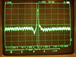 10T Near-Threshold SRAM
 FinFET 7nm SRAM Design
 IMC SRAM Macro
 Sense Amplifier Layout
Start Your Cadence SRAM Project Today
Whether you need a standard 6T SRAM bitcell for VTU, an 8T write-assist design for Anna University MTech, a FinFET stability analysis for a PhD thesis or a full IMC SRAM macro for an IEEE paper — our Cadence VLSI experts in Bangalore will guide you from schematic to DRC/LVS-clean layout, Monte-Carlo yield and post-layout simulation.