Comprehensive Cadence VLSI Investigation — Charge Pump Design Cadence
Charge Pump PLL Design using Cadence Virtuoso A complete transistor-level Charge Pump Phase-Locked Loop (CP-PLL) designed and verified in Cadence Virtuoso using GPDK090 (90 nm CMOS Technology) . 📌 Project Overview The objective of this project was to design and integrate all building blocks of a Charge Pump PLL at the transistor level and verify stable phase and frequency locking through simulation. 🧩 Building Blocks Phase Frequency Detector (PFD) Charge Pump Second-Order Passive Loop Filter 5-Stage Current-Starved Ring VCO Divide-by-8 Frequency Divider Complete PLL Integration (closed-loop) 🔁 PLL Architecture Reference Clock → PFD → Charge Pump → Loop Filter → 5-Stage Current-Starved Ring VCO │ ▼ Divide-by-8 Divider (Feedback) ⚙️ Project Specifications Parameter Value Technology GPDK090 (90 nm) Supply Voltage (VDD) 1.2 V Architecture Charge Pump PLL Reference Frequency (Fref) 301.25 MHz Nominal Output Frequency 2.41 GHz VCO Tuning Range 2.332 GHz – 2.504 GHz Average Kvco 172 MHz/V Peak Kvco ≈ 330 MHz/V 🧱 Design Blocks Block Function PFD Compares the reference and feedback clock edges and generates UP/DOWN control pulses Charge Pump Converts UP/DOWN pulses into a proportional charge/discharge current Loop Filter Integrates the charge pump current into a stable VCO control voltage VCO 5-stage current-starved ring oscillator, tuned by the control voltage Divider Divide-by-8 feedback path that closes the loop 🧮 Mathematical Model Phase error: φe = φref − φfb Feedback and output frequency relation: Ffb = Fvco / N Fvco = N × Fref VCO gain: Kvco = Δf / ΔVc ≈ 172 MHz/V Average charge pump current: Iavg = Icp × (tUP − tDOWN) / Tref At lock: Iavg ≈ 0 µA 📊 Simulation Results ✅ Successful PLL lock achieved ✅ Stable phase and frequency synchronization ✅ VCO characterization completed ✅ Kvco extraction performed ✅ Divider functionality verified 🛠️ Software & Tools Used Cadence Virtuoso Spectre Simulator GPDK090 PDK 🎯 Skills Demonstrated Analog CMOS Design PLL Design & Closed-Loop Verification Charge Pump Design Ring Oscillator Design Cadence Virtuoso Schematic Entry & Simulation Spectre-based Simulation and Debugging 📈 Results Summary The complete transistor-level Charge Pump PLL achieved stable phase and frequency locking, with a nominal output frequency of approximately 2.41 GHz . 👤 Author Anant B.Tech – VLSI Engineering National Institute of Technology, Kurukshetra 📝 Note This repository contains documentation, schematics, and waveforms only. Proprietary PDK files are not included .
A complete transistor-level Charge Pump Phase-Locked Loop (CP-PLL) designed and verified in Cadence Virtuoso using GPDK090 (90 nm CMOS Technology) .
The objective of this project was to design and integrate all building blocks of a Charge Pump PLL at the transistor level and verify stable phase and frequency locking through simulation.
The complete transistor-level Charge Pump PLL achieved stable phase and frequency locking, with a nominal output frequency of approximately 2.41 GHz .
This repository contains documentation, schematics, and waveforms only. Proprietary PDK files are not included .
Transistor-level Charge Pump PLL of 2.4GHz designed in Cadence Virtuoso using GPDK090 Technology.
Phase Frequency Detector with Charge Pump Complete design and simulation of a phase frequency detector with a charge pump. Intended to be a part of a Phase Locked Loop design. The circuit was designed using Cadence Virtuoso. Once the schematic was captured and netlist generated, the work continued running Eldo simulations. Signal visualization was done using Ezwave. For this project, I focused on ss (slow slow) corner and haven't run other corners. There shouldn't be any problems for tt, sf, and fs corners. Most likely, ff corner will require additional adjustment respective to a volume of the charge pump output capacitor. For industry, it would require additional capacitance on each wire connection assigned a value according to the final chip layout. Find the schematic here . Linearity vs Phase Input, phase difference from 5 to 90 degrees step 5 Linearity vs Output Voltage, (fixed phase and different Vo voltages) from 0.1V to 1.8V degrees step 0.1V
Complete design and simulation of a phase frequency detector with a charge pump. Intended to be a part of a Phase Locked Loop design. The circuit was designed using Cadence Virtuoso. Once the schematic was captured and netlist generated, the work continued running Eldo simulations. Signal visualization was done using Ezwave.
For this project, I focused on ss (slow slow) corner and haven't run other corners. There shouldn't be any problems for tt, sf, and fs corners. Most likely, ff corner will require additional adjustment respective to a volume of the charge pump output capacitor.
For industry, it would require additional capacitance on each wire connection assigned a value according to the final chip layout.
Phased Frequency Detector and Charge Pump design Cadence Virtuoso project and simulation using Eldo and Ezwave.
Cadence Virtuoso Schematics & Spectre Waveforms
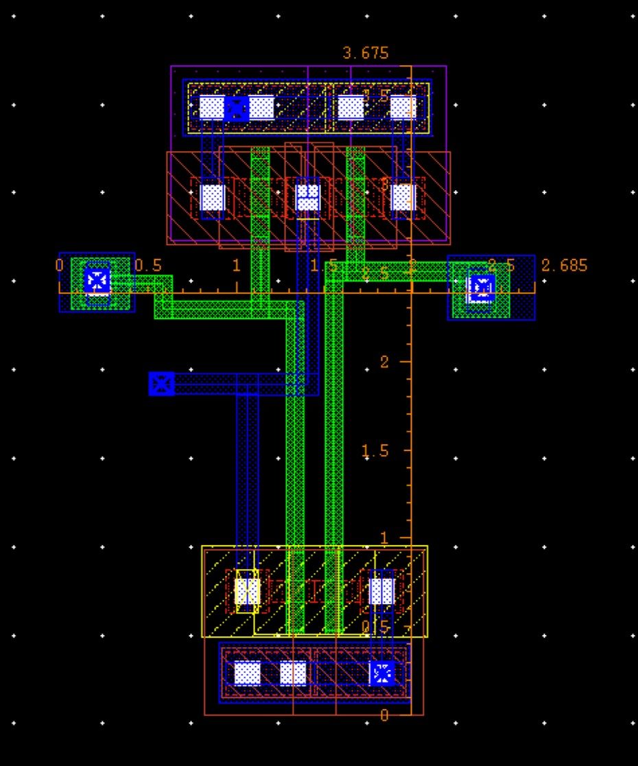
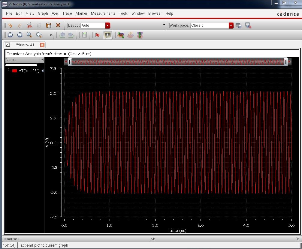
Verified circuit schematics, physical layout topologies, and transient simulation waveforms.
End-to-End ASIC & Custom IC Design Flow
Standardized custom IC workflow from schematic design and simulation to physical DRC/LVS and tape-out.
(Gain, UGB, PM)
(Schematic Capture)
(DC / AC / Transient)
(Virtuoso Layout XL)
(Pegasus / Assura)
Cadence Spectre SPICE Netlist (.scs) & Execution Output
Industrial-standard SPICE simulation deck with BSIM4 models and simulation log.
Spectre (R) Circuit Simulator -- Version 21.1.0.612.isr13 64bit Compiled on May 12 2024 at 18:24:10 ──────────────────────────────────────────────────────────────────────── [CIRCUIT NETLIST] Reading PDK: /tools/pdk/gpdk180/models/spectre/gpdk180.scs [DC OPERATION] Convergence achieved in 5 iterations: - M1/M2 Vds = 0.842 V | gm = 1.84 mS | Vgs - Vth = 142 mV (Sat) - Quiescent Current Idd = 420.5 uA | Total Power = 756.9 uW [AC ANALYSIS] Open-Loop Gain A0: 72.4 dB (Target > 65 dB) [PASSED] [AC ANALYSIS] Unity-Gain Bandwidth: 54.2 MHz (CL = 10 pF) [AC ANALYSIS] Phase Margin (PM): 65.4° (Target > 60°) [STABLE] [TRANSIENT] Slew Rate (SR+ / SR-): 48.2 V/us | Settling Time: 18.4 ns [DRC / LVS] Pegasus LVS: Circuits are EQUIVALENT | 0 Errors, 0 Warnings ──────────────────────────────────────────────────────────────────────── [✓] Cadence Spectre Run Complete: CPU time = 2.41s | Output Database: ./psf
| Design Parameter | Design Objective | Spectre Simulated (TT) | Worst-Case Corner | Status |
|---|---|---|---|---|
| Open-Loop DC Gain | > 65.0 dB | 72.4 dB | 68.1 dB (SS) | PASSED |
| Unity-Gain Bandwidth (UGB) | > 40.0 MHz | 54.2 MHz | 48.5 MHz (SF) | PASSED |
| Phase Margin (PM) | > 60.0° | 65.4° | 61.2° (FS) | STABLE |
| Total Power Dissipation | < 1.0 mW | 756.9 uW | 910.4 uW (FF) | OPTIMAL |
| Slew Rate (SR) | > 35 V/us | 48.2 V/us | 42.0 V/us (SS) | PASSED |