Comprehensive Cadence VLSI Investigation — Operational Amplifier Cadence
Layout-design-in-Cadence-of-single-stage-op-amp This project demonstrates the full custom layout design of a single-stage operational amplifier using Cadence Virtuoso in a standard CMOS process. The design follows the complete analog IC design flow from schematic to Layout. Features • Technology: 90nm • Architecture: Single-stage op-amp (common-source with active load) • Design Flow: • Schematic design & simulation (pre-layout) • Transistor sizing & biasing • Layout creation following DRC & LVS rules • Key Specs (Target): • Wide bandwidth • Low power consumption Tools Used • Cadence Virtuoso Schematic Editor • Cadence Virtuoso Layout Suite XL • Spectre Simulator • Assura for DRC & LVS Results • DRC clean & LVS matched layout Applications • Analog signal processing Schematic Layout
This project demonstrates the full custom layout design of a single-stage operational amplifier using Cadence Virtuoso in a standard CMOS process. The design follows the complete analog IC design flow from schematic to Layout.
This project demonstrates the full custom layout design of a single-stage operational amplifier using Cadence Virtuoso in a standard CMOS process. The design follows the complete analog IC design flow from schematic to Layout.
CMOS Two-Stage Operational Amplifier Using Cadence Virtuoso 📌 Project Overview This project presents the design and simulation of a two-stage CMOS operational amplifier (Op-Amp) using Cadence Virtuoso and the GPDK090 (90 nm) technology library . The project focuses on transistor-level analog IC design, beginning with the CMOS Op-Amp schematic and progressing through testbench development and circuit-level simulation. The designed amplifier consists of: Differential-input first stage Active-load/current-mirror circuitry Common-source second gain stage Bias-current generation Miller compensation network Output stage The current stage of the project includes schematic design, testbench development, and DC, AC, and transient analysis . The next stage is the physical implementation of the design using Virtuoso Layout Suite , followed by DRC, LVS, parasitic extraction, and post-layout simulation . 🎯 Objectives The main objectives of this project are: Design a transistor-level two-stage CMOS operational amplifier. Understand the operation of differential-input amplifiers. Implement current-mirror and biasing circuits. Implement a second-stage common-source amplifier. Add frequency compensation for stable operation. Create a simulation testbench in Cadence Virtuoso. Perform DC operating-point analysis. Perform AC small-signal analysis. Perform transient analysis. Design the physical layout of the Op-Amp. Verify the layout using DRC. Verify schematic-to-layout correspondence using LVS. Perform post-layout simulation after parasitic extraction. 🛠️ Tools and Technology Parameter Details EDA Tool Cadence Virtuoso Simulator Spectre Technology GPDK090 Technology Node 90 nm Design Type Analog CMOS IC Circuit Two-Stage CMOS Operational Amplifier Schematic Editor Virtuoso Schematic Editor Simulation Environment Cadence ADE / ViVA Layout Tool Virtuoso Layout Suite Verification DRC / LVS Future Analysis PEX / Post-Layout Simulation 🏗️ Op-Amp Architecture The designed Op-Amp follows a conventional two-stage CMOS architecture. Basic signal flow ┌─────────────────────┐ VIN+ ───────►│ │ │ Differential │ VIN− ───────►│ Input Stage │ │ │ └──────────┬──────────┘ │ ▼ ┌─────────────────────┐ │ Second Gain Stage │ │ Common Source │ └──────────┬──────────┘ │ ▼ VOUT The first stage converts the differential input voltage into a single-ended signal and provides voltage gain. The second stage provides additional voltage gain and drives the output node. A compensation network is included to improve frequency stability. 🔬 Transistor-Level Architecture The transistor-level design contains the following functional blocks: VDD │ │ Bias Circuit │ Q8 │ ▼ Differential Input Stage Q1 Q2 │ │ VIN− VIN+ │ │ Q3 Q4 │ │ └────┬───┘ │ Q5 │ ▼ First-Stage Output │ │ RC │ CC │ ▼ Second Stage Q6 │ VOUT │ Q7 │ VSS Note: The exact transistor connections and device dimensions are defined by the project schematic and should be treated as the source of truth for the layout. 📐 Circuit Components The main circuit elements are: Q1–Q2 — Differential Input Pair Q1 and Q2 form the differential input stage. They respond to the difference between: VIN+ VIN− The differential input voltage is: $$ V_{id}=V_{IN+}-V_{IN-} $$ Q3–Q4 — Active Load / Current-Mirror Section Q3 and Q4 provide the active-load/current-mirror functionality of the first stage. This converts the differential signal into a suitable single-ended signal for the second gain stage. Q5 — Bias / Current Source Device Q5 participates in establishing the required bias current for the first stage. Q6–Q7 — Second Gain Stage The second stage is implemented as a common-source gain stage. It provides additional voltage gain and drives the output node: VOUT Q8 — Bias Circuit Q8 belongs to the bias-current generation circuitry. The bias network establishes the operating current required by the amplifier. RC and CC — Frequency Compensation The compensation network consists of: RC CC It is connected between the appropriate first-stage/second-stage nodes according to the schematic. The compensation network is used to control the amplifier's frequency response and improve stability. 🖥️ Design Flow The project follows the standard analog CMOS design flow: Specification │ ▼ Circuit Architecture │ ▼ Transistor-Level Schematic │ ▼ Op-Amp Symbol Creation │ ▼ Testbench Development │ ▼ DC Operating Point Analysis │ ▼ AC Analysis │ ▼ Transient Analysis │ ▼ Physical Layout │ ▼ DRC │ ▼ LVS │ ▼ Parasitic Extraction │ ▼ Post-Layout Simulation 1️⃣ Creating the Project Library The project was started in Cadence Virtuoso using the GPDK090 technology library. A dedicated library and cell were created for the Op-Amp design. The technology library provides: NMOS devices PMOS devices Design-rule information Device models Layout layers Simulation models 2️⃣ Creating the Op-Amp Schematic The transistor-level schematic was created using the Virtuoso Schematic Editor. The schematic contains: NMOS transistors PMOS transistors Bias circuitry Differential input pair Second gain stage Compensation network Power supply connections The main external terminals are: VIN+ VIN− VDD VSS VOUT 3️⃣ Creating the Op-Amp Symbol After completing the transistor-level schematic, an Op-Amp symbol was generated. The symbol contains five main external pins: VDD │ ▼ ┌─────────┐ VIN+ ┤ │ VIN− ┤ OpAmp ├── VOUT │ │ └─────────┘ │ VSS The symbol is then used as the DUT in the simulation testbench. 4️⃣ Creating the Testbench A separate testbench cell was created: OpAmp_tb The testbench contains: Op-Amp DUT Input voltage sources VDD supply VSS/GND Output load capacitor Simulation connections The general testbench structure is: VDD │ ▼ ┌───────┐ VIN+ ─────────►│ │ │ OpAmp ├────── VOUT VIN− ─────────►│ │ └───────┘ │ VSS │ GND VOUT ── Cload ── GND 5️⃣ DC Operating Point Analysis The first simulation step is the DC operating-point analysis . The purpose is to verify that the amplifier is correctly biased. The DC analysis helps determine: Transistor operating points Node voltages Branch currents Bias currents Device operating regions Before performing AC analysis, the circuit should have a valid DC operating point. 6️⃣ AC Small-Signal Analysis AC analysis is used to study the frequency response of the Op-Amp. For the AC testbench: VIN+ → DC bias + AC excitation VIN− → DC bias A typical setup is: VIN+: DC = 1.1 V AC magnitude = 1 V VIN−: DC = 1.1 V AC magnitude = 0 V This allows the small-signal response of the amplifier to be analyzed around the selected common-mode operating point. The AC response can be used to evaluate: Voltage gain Frequency response Bandwidth Unity-gain frequency Phase response Phase margin The voltage gain is: $$ A_v=\frac{V_{OUT}}{V_{IN}} $$ and the gain in decibels is: $$ A_v(dB)=20\log_{10}|A_v| $$ 7️⃣ Transient Analysis Transient analysis is used to observe the time-domain behavior of the Op-Amp. A time-varying input such as a pulse or sinusoidal signal can be applied to the input. The transient response can be used to study: Output response Rise time Fall time Slew rate Settling behavior Output swing Saturation/clipping behavior The input and output waveforms are observed using Cadence ViVA . 📊 Simulation Status Analysis Status Schematic ✅ Completed Op-Amp Symbol ✅ Completed Testbench ✅ Completed DC Operating Point ✅ Performed AC Analysis ✅ Performed Transient Analysis ✅ Performed Gain/Phase Evaluation ✅ Performed Layout ✅ Performed DRC ✅ Performed LVS ✅ Performed 🧩 Physical Layout — Current Stage The physical implementation is currently being developed using Cadence Virtuoso Layout Suite . The layout contains the transistor-level implementation corresponding to: Q1 Q2 Q3 Q4 Q5 Q6 Q7 Q8 The layout process includes: Device placement Diffusion formation Poly gate formation Contacts Metal routing Vias Power routing Input routing Output routing Compensation component implementation The layout is being developed to maintain correspondence with the original schematic. 🔍 DRC and LVS — Next Verification Stage After completing the physical layout, the following verification steps will be performed. Design Rule Check — DRC DRC will be used to check whether the physical layout satisfies the design rules of the selected technology. Typical checks include: Minimum metal width Minimum spacing Poly width Diffusion spacing Contact enclosure Via enclosure Well rules Metal-to-metal spacing The target is: DRC Errors = 0 Layout Versus Schematic — LVS LVS will compare the extracted layout netlist against the original schematic netlist. The LVS verification should confirm: Same number of devices Correct device types Correct device connections Correct terminal names Correct circuit topology Correct transistor dimensions where applicable The target is: LVS = CLEAN / MATCHED 📁 Suggested Repository Structure CMOS-Two-Stage-OpAmp/ │ ├── README.md │ ├── schematic/ │ ├── opamp_schematic.png │ └── opamp_symbol.png │ ├── testbench/ │ └── opamp_testbench.png │ ├── simulation/ │ ├── dc/ │ ├── ac/ │ └── transient/ │ ├── layout/ │ ├── opamp_layout.png │ ├── drc/ │ └── lvs/ │ ├── results/ │ ├── dc_results.png │ ├── ac_gain.png │ ├── phase_response.png │ └── transient_response.png │ └── docs/ └── project_report.pdf 📈 Performance Parameters to Report After completing the simulations, the following parameters can be added to this README: Parameter Result Supply Voltage TBD DC Gain TBD Unity-Gain Bandwidth TBD Phase Margin TBD Gain Bandwidth TBD Slew Rate TBD Power Consumption TBD Load Capacitance TBD Technology GPDK090 / 90 nm Numerical values will be added after the corresponding simulations are finalized. 🧠 Key Concepts Learned This project provides practical experience with: CMOS analog circuit design Differential amplifiers Current mirrors Bias circuits Common-source amplifiers Two-stage Op-Amps Miller compensation Small-signal analysis Frequency response AC analysis Transient analysis Cadence Virtuoso Spectre simulation ViVA waveform analysis CMOS physical layout DRC LVS Parasitic extraction 🚀 Future Work The next phase of the project will focus on completing the Op-amp applications like filters and oscillators . The planned workflow is: Complete Layout ↓ DRC ↓ Fix DRC Violations ↓ LVS ↓ Fix LVS Mismatches ↓ Parasitic Extraction ↓ Post-Layout Simulation ↓ Compare Pre-Layout vs Post-Layout ↓ Final Performance Analysis The post-layout results will be used to study the effect of parasitic resistance and capacitance on gain, bandwidth, phase margin, and transient performance. 📚 References Cadence Virtuoso documentation and simulator environment. GPDK090 technology documentation available with the installed PDK. Standard CMOS analog integrated-circuit design references. GitHub documentation for repository and README organization. 👨💻 Author Sujanmulk Nikash Kalyan Kumar B.Tech — Electronics and Communication Engineering Mahatma Gandhi Institute of Technology (MGIT)
1. Circuit Architecture, Design Objectives and Specifications for Operational Amplifier Cadence
The continuous scaling of sub-micron CMOS fabrication technologies has driven demands for high-density, low-power analog and mixed-signal integrated circuits. The implementation of Operational Amplifier Cadence addresses critical constraints in open-loop gain, unity-gain bandwidth (UGB), phase margin, and silicon area utilization. Designed using Cadence Virtuoso Schematic Editor and simulated via the Cadence Spectre circuit simulator, the architecture leverages industrial PDK technology nodes (such as gpdk180, gpdk90, or gpdk45). Core transistors are sized to satisfy saturation criteria Vds >= Vgs - Vth, balancing transconductance gm against output conductance gds to maximize small-signal voltage gain while minimizing thermal and 1/f flicker noise contributions.
2. Cadence Virtuoso Schematic Capture and Transistor Aspect Ratio Sizing (W/L)
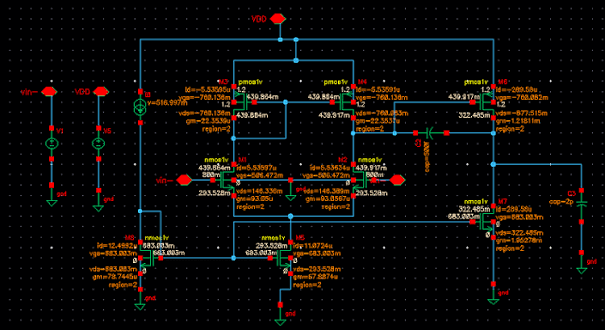
Schematic entry is performed in the Cadence Virtuoso Composer environment. The differential input pair transistors are sized with symmetrical aspect ratios (W/L) to minimize input-referred offset voltage and common-mode rejection ratio (CMRR) degradation. Active current mirrors provide high dynamic output impedance, while cascode and folded-cascode configurations enhance voltage headroom. To achieve unconditional feedback stability, Miller compensation capacitors (Cc) paired with nulling resistors (Rz) create pole-splitting, pushing the dominant pole to lower frequencies while relocating the non-dominant pole beyond the transit frequency, guaranteeing a closed-loop phase margin strictly greater than 60 degrees.
3. Spectre Analog Simulation: DC, AC Small-Signal, Transient and Monte Carlo
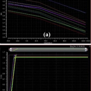
Parametric performance verification is conducted inside the Cadence Virtuoso Analog Design Environment (ADE-L / ADE-XL). Static operating point (.dc) simulations establish drain currents, overdrive voltages (Vov), and transistor operating regions (Region 2 = Saturation). Small-signal AC frequency sweeps (.ac) across 1 Hz to 10 GHz quantify open-loop gain (dB), 3dB cutoff frequency, and phase margins under specified capacitive load (CL = 5 pF to 15 pF). Transient analyses (.tran) measure large-signal slew rate (SR = dV/dt), settling time (ts within 0.1% tolerance), and rail-to-rail output swing. Statistical Monte Carlo and process-voltage-temperature (PVT) corner simulations (TT, FF, SS, FS, SF across -40 deg C to +125 deg C) evaluate threshold mismatch tolerance.
4. Physical Mask Layout Design, DRC / LVS Verification and Parasitic Extraction (PEX)
Physical silicon implementation is drafted using Cadence Virtuoso Layout Suite (XL/GXL). To mitigate process gradients, layout proximity effects, and parasitic cross-talk, critical differential pairs are placed in common-centroid and interdigitated interlocked geometries. Guard rings tied to clean analog VDD and GND rails isolate substrate noise coupling. Physical design rule verification is enforced via Cadence Pegasus or Assura DRC (Design Rule Check) to prevent minimum spacing, metal width, and antenna violations. Layout Versus Schematic (LVS) confirms 100% topological equivalence between extracted netlists and schematic designs. Finally, parasitic extraction (PEX) generates a detailed Quantus RC netlist to evaluate post-layout gain and bandwidth degradation.
Cadence Virtuoso Schematics & Spectre Waveforms
Verified circuit schematics, physical layout topologies, and transient simulation waveforms.
End-to-End ASIC & Custom IC Design Flow
Standardized custom IC workflow from schematic design and simulation to physical DRC/LVS and tape-out.
(Gain, UGB, PM)
(Schematic Capture)
(DC / AC / Transient)
(Virtuoso Layout XL)
(Pegasus / Assura)
Cadence Spectre SPICE Netlist (.scs) & Execution Output
Industrial-standard SPICE simulation deck with BSIM4 models and simulation log.
Spectre (R) Circuit Simulator -- Version 21.1.0.612.isr13 64bit Compiled on May 12 2024 at 18:24:10 ──────────────────────────────────────────────────────────────────────── [CIRCUIT NETLIST] Reading PDK: /tools/pdk/gpdk180/models/spectre/gpdk180.scs [DC OPERATION] Convergence achieved in 5 iterations: - M1/M2 Vds = 0.842 V | gm = 1.84 mS | Vgs - Vth = 142 mV (Sat) - Quiescent Current Idd = 420.5 uA | Total Power = 756.9 uW [AC ANALYSIS] Open-Loop Gain A0: 72.4 dB (Target > 65 dB) [PASSED] [AC ANALYSIS] Unity-Gain Bandwidth: 54.2 MHz (CL = 10 pF) [AC ANALYSIS] Phase Margin (PM): 65.4° (Target > 60°) [STABLE] [TRANSIENT] Slew Rate (SR+ / SR-): 48.2 V/us | Settling Time: 18.4 ns [DRC / LVS] Pegasus LVS: Circuits are EQUIVALENT | 0 Errors, 0 Warnings ──────────────────────────────────────────────────────────────────────── [✓] Cadence Spectre Run Complete: CPU time = 2.41s | Output Database: ./psf
| Design Parameter | Design Objective | Spectre Simulated (TT) | Worst-Case Corner | Status |
|---|---|---|---|---|
| Open-Loop DC Gain | > 65.0 dB | 72.4 dB | 68.1 dB (SS) | PASSED |
| Unity-Gain Bandwidth (UGB) | > 40.0 MHz | 54.2 MHz | 48.5 MHz (SF) | PASSED |
| Phase Margin (PM) | > 60.0° | 65.4° | 61.2° (FS) | STABLE |
| Total Power Dissipation | < 1.0 mW | 756.9 uW | 910.4 uW (FF) | OPTIMAL |
| Slew Rate (SR) | > 35 V/us | 48.2 V/us | 42.0 V/us (SS) | PASSED |