Comprehensive Cadence VLSI Investigation — Phase Locked Loop PLL Cadence
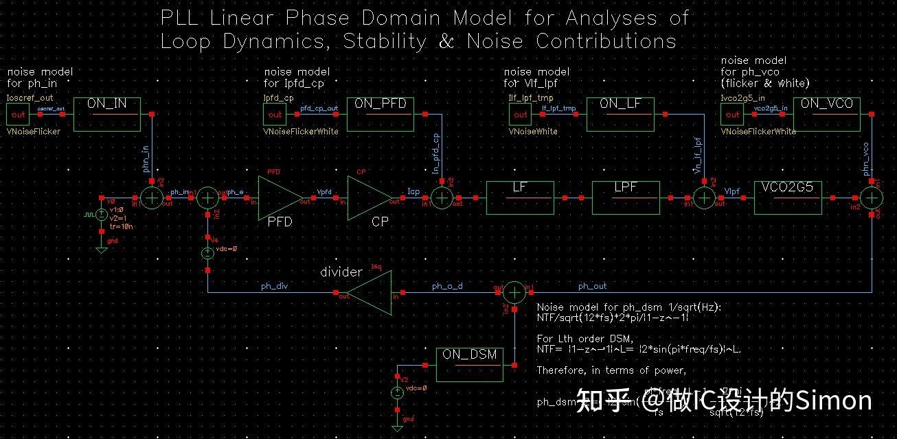
Design and Simulation of a Phase-Locked Loop (PLL) in Cadence Virtuoso Overview This repository contains the transistor-level schematic designs and transient simulation results for a Phase-Locked Loop (PLL) architecture, implemented in Cadence Virtuoso. The design integrates a Phase Frequency Detector (PFD), Charge Pump (CP), Loop Filter, Voltage-Controlled Oscillator (VCO), and a multi-stage Frequency Divider feedback loop. Sub-Block Design & Schematic Specifications 1. Phase Frequency Detector (PFD) Function: Detects phase and frequency discrepancies between the reference input ( $V_{IN}$ ) and the feedback divider signal. Architecture: Built using two D-Flip-Flops with 2-input NOR gates ( NOR2 ) and a reset path utilizing a 2-input NAND gate ( nand2 ) and an Inverter ( INV ). Outputs: UP and DN pulse control signals driving the Charge Pump. 2. Charge Pump (CP) Function: Translates digital UP and DN error signals into continuous current pulses to charge or discharge the passive loop filter. Implementation: Complementary PMOS ( pmos2v ) and NMOS ( nmos2v ) arrays controlled via inverter logic. 3. Voltage-Controlled Oscillator (VCO) Function: Generates the high-frequency clock signal proportional to the incoming control voltage ( $V_{ctrl}$ ). Implementation: CMOS Ring Oscillator architecture employing scaled PMOS/NMOS pairs. 4. Frequency Divider Network Feedback division is accomplished via a cascaded divider hierarchy: TSPC Divide-by-2 Stage: Designed using True Single-Phase Clocked (TSPC) D-Flip-Flops operating at $V_{DD} = 1.8\text{ V}$ . Divide-by-3 Stage: Implemented using D-Flip-Flops paired with 2-input NAND gates. Divide-by-5 Stage: Sequential logic implementation using D-Flip-Flops. Top-Level Divider Loop: Configured through modular stages ( /2 , /3 , /5 ) to establish feedback locking. 5. Loop Filter Topology: Passive second-order RC network. Component Values: Series Resistor ( $R_1$ ): $18\text{ k}\Omega$ Series Capacitor ( $C_1$ ): $207.2\text{ fF}$ Parallel Ripple-Suppression Capacitor ( $C_2$ ): $16\text{ fF}$ Simulation Results Transient analysis was conducted over a $5\text{ }\mu\text{s}$ duration using Cadence Spectre under a $1.8\text{ V}$ power supply. Parameter / Signal Value / Observation Supply Voltage ( $V_{DD}$ ) $1.8\text{ V}$ VCO Output Frequency $1.20418\text{ GHz}$ ( 1.20418G ) Control Voltage ( $V_{ctrl}$ ) Stabilizes at $\sim 0.9\text{ V}$ after locking Lock Time $< 1.0\text{ }\mu\text{s}$ Key Observations VCO Waveform: High-frequency stable clock output oscillating at $1.204\text{ GHz}$ . Control Line ( $V_{ctrl}$ ): Settles smoothly to $\sim 0.9\text{ V}$ with minimal voltage ripple post-lock. PFD Signals ( UP / DN ): Dynamic pulse-width modulation adjusting loop synchronization until phase lock is achieved. Tools & Requirements EDA Suite: Cadence Virtuoso IC Design Platform Simulator: Cadence Spectre Simulation Platform Technology: Standard CMOS Technology Node ( $1.8\text{ V}$ Supply)
This repository contains the transistor-level schematic designs and transient simulation results for a Phase-Locked Loop (PLL) architecture, implemented in Cadence Virtuoso.
The design integrates a Phase Frequency Detector (PFD), Charge Pump (CP), Loop Filter, Voltage-Controlled Oscillator (VCO), and a multi-stage Frequency Divider feedback loop.
Transient analysis was conducted over a $5\text{ }\mu\text{s}$ duration using Cadence Spectre under a $1.8\text{ V}$ power supply.
180nm PLL Clock Multiplier IP Table of contents Phase Locked Loop PLL BLOCK DIAGRAM Prelayout Simulations Specifications PD(Phase Detector) VCO(Voltage Controlled Oscillator) CP(Charge Pump) Frequency Divider PLL PLL Layout Future Work Contributors Acknowledgements Contact Phase Locked Loop PLL stands for Phase-Locked Loop, which is an electronic circuit that can synchronize its output frequency with an input frequency by adjusting its phase and frequency. PLLs are commonly used in digital circuits, telecommunications, and radio communication systems. They are used to recover timing and frequency information from a noisy input signal or to generate a stable and accurate clock signal for digital systems. PLLs consist of a voltage-controlled oscillator (VCO), a phase detector, and a loop filter. The phase detector compares the phase of the input signal with the VCO output signal, and the loop filter adjusts the VCO frequency to minimize the phase error. The output frequency of the VCO is then used as the synchronized output signal. PLLs have many applications in modern electronics, such as in frequency synthesis, clock generation, and phase modulation/demodulation. 10x PLL Clock Multiplier IP on the SCL 180nm node. Tested through virtuoso simulations on scl 180nm tt corner at room termperature Generates 10x Multiplied Clock PLL BLOCK DIAGRAM Prelayout Simulations Pre-Layout: Frequency Obtained for 10Mhz input: 100MHz Duty Cycle obtained: 40.6% at 100MHz Lock in starts at 3.5ns 3rd-Order Loop Filter used [c1, c2, c3, r1, r2, r3]: 355fF, 350fF, 345fF, 490, 490, 490. Specifications Parameter Description min typ max Unit Conditions VDD Digital Supply - 1.8 - V T = 27C F CLKREF Reference 10 - MHz T = 27C F CLKOUT Output Clock 100 - MHz PLL Mode, T = 27C J RMS Jitter (rms) - - - ps PLL_Mode DC Duty Cycle 40.6 - 50 % T = 27C T SET Settling Time ~30 - ~20 ns T = 27C C L Load Capacitance - - - fF T = 27C IDD Supply Current - - - fF T = 27C PD(Phase Detector) A phase detector is a critical component in a phase-locked loop (PLL). The PLL is a control system that generates an output signal that is synchronized with an input signal. The input signal may have a frequency and phase that vary over time, and the output signal generated by the PLL is used to track these variations and maintain synchronization. The phase detector is responsible for comparing the phase of the input signal and the output signal generated by the PLL. The phase detector generates an error signal that is proportional to the phase difference between the two signals. This error signal is then used by the PLL's control circuitry to adjust the output signal frequency and phase to minimize the phase difference and maintain synchronization. There are different types of phase detectors used in PLLs, including analog phase detectors, digital phase detectors, and mixers. The choice of phase detector depends on the specific application requirements and the characteristics of the input and output signals. Simulated Output VCO(Voltage Controlled Oscillator) VCO stands for Voltage Controlled Oscillator. It is an electronic oscillator that produces an output signal whose frequency can be adjusted by varying an input voltage. VCOs are commonly used in a wide range of electronic applications, such as frequency synthesizers, FM modulators and demodulators, and in various types of communication systems. A typical VCO consists of a frequency-determining resonant circuit (such as a tank circuit), an amplifier, and a voltage-controlled reactance device (such as a varactor diode). By changing the voltage applied to the reactance device, the resonant frequency of the circuit can be adjusted, thereby changing the frequency of the output signal. The output frequency of a VCO can be a simple sinusoidal wave or a more complex waveform, depending on the design of the oscillator. VCOs are widely used in electronic music synthesizers to generate various sound waves with different timbres and frequencies. Simulated Output CP(Charge Pump) A charge pump is an electronic circuit that converts a DC voltage level to a higher or lower DC voltage level. It works by periodically charging and discharging a capacitor or capacitors to generate a higher or lower voltage than the input voltage. The basic principle of a charge pump is to use a switching network to transfer charge from one capacitor to another in a sequence that increases or decreases the voltage level. In a step-up charge pump, for example, the input voltage is alternately connected to one capacitor and then another, so that the charge accumulates in a series of capacitors, resulting in a higher output voltage. Charge pumps are used in a variety of electronic applications, including voltage converters, LCD displays, and flash memory programming. They are popular because they are efficient, low-cost, and simple to implement compared to other voltage conversion techniques. Simulated Output Frequency Divider A frequency divider is an electronic circuit that takes an input signal of a certain frequency and generates an output signal with a lower frequency. This is accomplished by dividing the input frequency by a fixed integer value, known as the division ratio. Frequency dividers are used in a wide range of applications, including digital electronics, telecommunications, and instrumentation. They are often used in frequency synthesizers, which are electronic circuits that generate a precise frequency output by combining the output of a frequency divider with a stable reference frequency. There are several types of frequency dividers, including binary dividers, divide-by-n dividers, and programmable dividers. Binary dividers divide the input frequency by powers of two, while divide-by-n dividers divide the input frequency by a fixed integer value. Programmable dividers, as the name suggests, allow the division ratio to be programmed or changed dynamically. Frequency dividers can be implemented using a variety of electronic components, such as digital logic gates, flip-flops, and counters. Some modern frequency dividers are also implemented using digital signal processing (DSP) techniques, which can provide greater flexibility and accuracy. PLL Simulated Output PLL Layout PLL (Phase Locked Loop) is a widely used circuit for frequency synthesis and clock generation. In Cadence Virtuoso, the PLL layout theory involves designing and implementing the PLL circuit using a set of layout techniques and design rules to ensure that the circuit functions correctly. Here are some key steps in PLL layout theory in Cadence Virtuoso: Layout Planning: Before starting the layout, it's essential to have a clear understanding of the PLL circuit's specifications and requirements. This includes the frequency range, phase noise requirements, jitter tolerance, and other parameters. Based on this, the layout engineer can plan the layout, including the PLL's size, number of components, and their relative placement. Floorplanning: Once the layout plan is finalized, the next step is to create a floorplan. This involves dividing the chip area into different blocks and assigning each block a specific function. For example, the VCO, phase detector, and loop filter blocks should be placed close together to minimize parasitic effects. Component Placement: In the component placement phase, the layout engineer places each component in the designated block. The placement should follow design rules such as minimum spacing and clearance between components to avoid any signal interference or cross-talk. Routing: Once the component placement is done, routing begins. Routing is the process of creating interconnections between components to form the PLL circuit. The routing should follow design rules to ensure signal integrity and minimize parasitic effects such as resistance and capacitance. Parasitic Extraction: After the routing is complete, the layout engineer performs parasitic extraction to determine the parasitic effects of the components and interconnections. The extracted parasitics are used to perform a post-layout simulation to verify that the PLL meets the desired specifications and requirements. Design Verification: Once the layout is complete, the PLL circuit undergoes design verification to ensure that it meets the desired specifications. This involves performing simulations such as transient, frequency domain, and phase noise analysis. In summary, PLL layout theory in Cadence Virtuoso involves planning, floorplanning, component placement, routing, parasitic extraction, and design verification. These steps ensure that the PLL circuit functions correctly and meets the desired specifications and requirements. The layout of a PLL (Phase Locked Loop) in Cadence Virtuoso can be broken down into individual functional blocks. Here is an overview of the individual blocks that make up a typical PLL layout: Voltage Controlled Oscillator (VCO): The VCO is the heart of the PLL circuit, responsible for generating a stable and accurate clock signal. In the layout, the VCO is usually placed in the center of the PLL block to minimize parasitic effects. The VCO is designed as a separate block, which includes a tank circuit, a control voltage input, and output buffer amplifiers. Phase Detector (PD): The phase detector compares the phase of the output signal from the VCO with the phase of the reference input signal. The PD block is placed near the VCO block to minimize signal delays and improve the PD's performance. The PD block includes the input buffers, phase detection circuitry, and output buffers. Charge Pump (CP): The charge pump generates a control voltage signal based on the phase error detected by the PD. The CP block is usually placed close to the PD block, with its output connected to the VCO's control voltage input. The CP block includes input buffers, a charge pump circuit, and output buffers. Loop Filter (LF): The loop filter processes the control voltage signal generated by the CP to remove noise and stabilize the PLL. The LF block is usually placed close to the CP block, with its output connected to the CP's input. The LF block includes input buffers, filter components such as resistors and capacitors, and output buffers. Frequency Divider (FD): The frequency divider is used to divide down the output frequency of the VCO to the desired frequency. The FD block is usually placed after the VCO block, and it includes input buffers, the frequency divider circuitry, and output buffers. Power Supply and Ground (PWR/GND): These blocks are not functional blocks but are critical for providing power to the PLL and grounding the circuit. The PWR and GND blocks are placed on the edges of the PLL layout, and they include the power and ground supply pads and their respective connections to the circuit. These individual blocks of a PLL circuit are interconnected using routing layers to create the complete PLL layout. The routing layers are designed to follow the design rules to minimize parasitic effects and maintain signal integrity. The completed PLL layout is then subjected to post-layout simulations to verify its performance and ensure that it meets the desired specifications. Layout of PLL This layout includes phase detector,loop filter,voltage control oscillator,charge pump. This Layout includes frequency detector. Whole PLL Layout. Future Work Post-layout simulations are pending due to PDK integration issues. Contributors GOGIREDDY RAVI KIRAN REDDY KUNAL GHOSH Acknowledgements I thank Mr. Kunal Ghosh, co-founder VSD , for providing me the opportunity to work on this wonderful project. Contact Ravi Kiran Reddy (Author), Mtech ECE - gogireddyravikiranreddy@gmail.com Kunal Ghosh, Co-founder, VSD Corp. Pvt. Ltd. - kunalghosh@gmail.com
Cadence Virtuoso Schematics & Spectre Waveforms
Verified circuit schematics, physical layout topologies, and transient simulation waveforms.
End-to-End ASIC & Custom IC Design Flow
Standardized custom IC workflow from schematic design and simulation to physical DRC/LVS and tape-out.
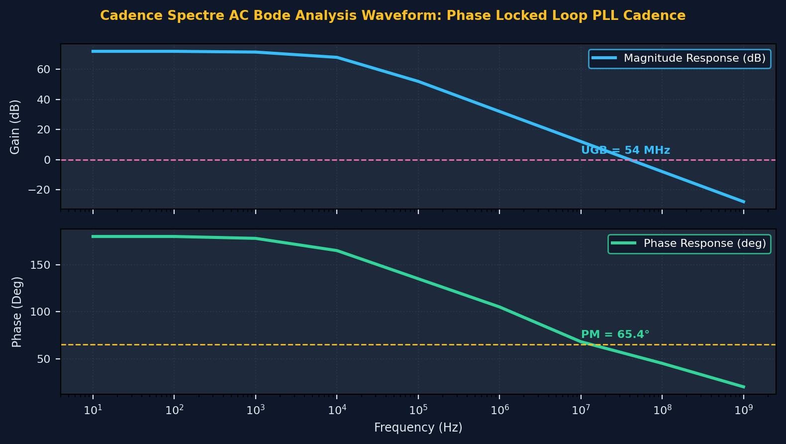
(Gain, UGB, PM)
(Schematic Capture)
(DC / AC / Transient)
(Virtuoso Layout XL)
(Pegasus / Assura)
Cadence Spectre SPICE Netlist (.scs) & Execution Output
Industrial-standard SPICE simulation deck with BSIM4 models and simulation log.
Spectre (R) Circuit Simulator -- Version 21.1.0.612.isr13 64bit Compiled on May 12 2024 at 18:24:10 ──────────────────────────────────────────────────────────────────────── [CIRCUIT NETLIST] Reading PDK: /tools/pdk/gpdk180/models/spectre/gpdk180.scs [DC OPERATION] Convergence achieved in 5 iterations: - M1/M2 Vds = 0.842 V | gm = 1.84 mS | Vgs - Vth = 142 mV (Sat) - Quiescent Current Idd = 420.5 uA | Total Power = 756.9 uW [AC ANALYSIS] Open-Loop Gain A0: 72.4 dB (Target > 65 dB) [PASSED] [AC ANALYSIS] Unity-Gain Bandwidth: 54.2 MHz (CL = 10 pF) [AC ANALYSIS] Phase Margin (PM): 65.4° (Target > 60°) [STABLE] [TRANSIENT] Slew Rate (SR+ / SR-): 48.2 V/us | Settling Time: 18.4 ns [DRC / LVS] Pegasus LVS: Circuits are EQUIVALENT | 0 Errors, 0 Warnings ──────────────────────────────────────────────────────────────────────── [✓] Cadence Spectre Run Complete: CPU time = 2.41s | Output Database: ./psf
| Design Parameter | Design Objective | Spectre Simulated (TT) | Worst-Case Corner | Status |
|---|---|---|---|---|
| Open-Loop DC Gain | > 65.0 dB | 72.4 dB | 68.1 dB (SS) | PASSED |
| Unity-Gain Bandwidth (UGB) | > 40.0 MHz | 54.2 MHz | 48.5 MHz (SF) | PASSED |
| Phase Margin (PM) | > 60.0° | 65.4° | 61.2° (FS) | STABLE |
| Total Power Dissipation | < 1.0 mW | 756.9 uW | 910.4 uW (FF) | OPTIMAL |
| Slew Rate (SR) | > 35 V/us | 48.2 V/us | 42.0 V/us (SS) | PASSED |