Comprehensive Cadence VLSI Investigation — Rtl To Gdsii Cadence Flow
بِسْمِ اللهِ الرَّحْمنِ الرَّحِيم “وَمَا أُوتِيتُمْ مِنَ الْعِلْمِ إِلَّا قَلِيلًا” Abstract This tutorial teaches how to implement a design idea from RTL-to-GDSII flow using Cadence® tools. You will learn how to deal with these challenges while running the flow, such as resolving errors in the log file, debugging the timing violations, and fixing setup and hold violations. After completing the lecture, you can download a lab database and manual to test your knowledge at every stage. After completing this tutorial, you will be able to: Code a design in Verilog as per the design specification provided Compile, elaborate, and simulate your design Synthesize your design Design for test Run equivalency checking at different stages of the flow Floorplan a design Run placement, optimization, clock tree synthesis, and routing on your design Run signoff checks to ensure that can able to fabricate a chip. Write out a GDSII file. Table of Contents Abstract Cadence-RTL-to-GDSII-FlowCadence-RTL-to-GDSII-Flow Counter Design Simulating a Simple Counter Design Synthesis Stage Equivalency Checking Stage Implementation Stage Gate-Level Simulation Stage Timing Analysis and Debug Stage Acknowledgements Reference Cadence-RTL-to-GDSII-Flow In this tutorial, you learn how to implement a design from RTL-to-GDSII using Cadence® tools. You will start by coding a design in Verilog. You will simulate the coded design, followed by design synthesis and optimization. You will then run equivalency checks at different stages of the flow. After synthesizing the design, you will floorplan, and place-and-route the synthesized netlist while meeting timing. You will run a gate-level simulation throughout the flow. Finally, you will write out a GDSII file The following is the directory structure of the counter design mini-project directory description RTL Contains common RTL design files Simulation Run Incisive simulation here Synthesis Run Genus synthesis here Equivalence Checking Run Conformal equivalence checking here GLS Run Incisive gate-level simulation here Constraints Constraints – Contains the SDC file physical_design Run Innovus implementation here STA Run Tempus timing analysis here LIB Contains lib files LEF Contains lef files QRC_tech Contains the QRC tech file Captable Captable – Contains the Cap table Run the different tools in separate directories so that all log files, command files, and other tool-generated files do not get mixed up. DO NOT modify the common directories like captable, constraints, lib, lef, QRC_Tech, and rtl. During your run, save your modified design files inside the same directory where you run those tools. Counter-Design The binary counter is an example of a simple synchronous digital circuit. It has no data inputs and no combinational output logic circuit. At each clock pulse, the counter takes up a new state and thus goes through a specific count sequence. We shall now write a design spec for 8bit up-counter with two outputs which go through the following sequence: The counter should have the following inputs: rst, which is synchronous, active low clk The counter should have the following output: count (7:0) Simulating-a-Simple-Counter-Design This lab uses the following software: Incisive 15.2 Go to the “simulation” directory: cd simulation You will see two files here: counter.v , which is the design itself, and counter_test.v , which is the testbench, both written in Verilog. Execute the following command: irun counter.v counter_test.v -access +rwc -gui & -access +rwc provides probing access to all the signals in the design hierarchy. -gui invokes the graphical mode of the NCSim tool Synthesis-Stage The tool used for synthesis (converting RTL to a gate-level netlist) is Genus™ Synthesis Solution (Genus) in Stylus Common UI mode This lab uses the following software: GENUS 17.1 Change to the synthesis directory by entering the following command: cd Synthesis Start the software in Stylus Common UI mode by entering: genus Use the following command to invoke Genus along with the script file: genus –f synthesis.tcl Equivalency-Checking-Stage The tool used for equivalence checking (comparing RTL to gate-level netlist) is the Conformal® Logic Equivalence Checker (LEC). Conformal LEC is a tool used for formal verification of designs at various stages in the flow. Formal verification is the process of verifying designs using mathematical methods. Equivalence Checking is the process of verifying the correctness of a modified or transformed design (revised design) by comparing it with a reference design (golden design). This lab uses the following software: CONFRML 17.1 Change the directory to Equivalence_checking. cd Equivalence_Checking Invoke Conformal LEC inside the Equivalence_checking directory in non-GUI by using the command: lec -XL -nogui -color -64 -dofile counter.do -XL : Launches Conformal L with Datapath and advanced equivalence checking capabilities. -nogui : Starts the session in non-GUI mode. -color : Turns on color-coded messaging when in non-GUI mode. -64 : Runs the Conformal software in 64-bit mode. -dofile < counter.do >: Runs the script < counter.do > after starting LEC. Implementation-Stage In this lab, you will use the Innovus™ Implementation System to implement the floorplanning, placement, routing, etc., for this design. At the end of the lab, you will also verify your results before handing them off for signoff. This lab uses the following software: INNOVUS 17.1 Change to the working directory where you will run floorplanning by entering: cd PnR Start the Innovus Implementation System by entering: innovus -stylus Gate-Level-Simulation-Stage This lab uses the following software: Incisive 15.2 Change to the working directory: cd GLS Execute the following xrun command: irun -timescale 1ns/10ps counter_netlist.v counter_test.v -v slow_vdd1v0_basicCells.v -access +rwc -define SDF_TEST -mess –gui -timescale : To mention the time unit and time precision. -access : Passed to the elaborator to provide read access to simulation objects. -gui : To invoke the xrun in gui mode. -mess : To display all the messages in detail. -define : To provide SDF definition present in the testbench. -v : To provide library in “.v” format. Timing-Analysis-and-Debug-Stage Tempus™ Timing Signoff Solution is a timing signoff tool used to verify that the design meets your timing goals. In this lab, you will first rerun the previous session of Place & Route and continue it with running Tempus timing analysis inside of Innovus™ This lab uses the following software: INNOVUS 17.1 Acknowledgements Nothing is done in isolation. I would like to thank Dr. Hesham Omran and Eng. Islam Samir for having made important contribution to this work. I am very grateful to my family for always being supportive of me. My parents, and my friends have been the shining light of my life. I was inspired by late Prof. Adam Teman, who taught a very different course on RTL2GDS at Bar-Ilan University. His design-oriented analysis approach seemed like the right mindset. Reference Digital VLSI Design (RTL to GDS) Digital IC Design (1) Digital IC Design (2) Digital IC Design (3) Cadence Documentation Ron Rutenbar “From Logic to Layout”
1. Circuit Architecture, Design Objectives and Specifications for Rtl To Gdsii Cadence Flow
The continuous scaling of sub-micron CMOS fabrication technologies has driven demands for high-density, low-power analog and mixed-signal integrated circuits. The implementation of Rtl To Gdsii Cadence Flow addresses critical constraints in open-loop gain, unity-gain bandwidth (UGB), phase margin, and silicon area utilization. Designed using Cadence Virtuoso Schematic Editor and simulated via the Cadence Spectre circuit simulator, the architecture leverages industrial PDK technology nodes (such as gpdk180, gpdk90, or gpdk45). Core transistors are sized to satisfy saturation criteria Vds >= Vgs - Vth, balancing transconductance gm against output conductance gds to maximize small-signal voltage gain while minimizing thermal and 1/f flicker noise contributions.
2. Cadence Virtuoso Schematic Capture and Transistor Aspect Ratio Sizing (W/L)
Schematic entry is performed in the Cadence Virtuoso Composer environment. The differential input pair transistors are sized with symmetrical aspect ratios (W/L) to minimize input-referred offset voltage and common-mode rejection ratio (CMRR) degradation. Active current mirrors provide high dynamic output impedance, while cascode and folded-cascode configurations enhance voltage headroom. To achieve unconditional feedback stability, Miller compensation capacitors (Cc) paired with nulling resistors (Rz) create pole-splitting, pushing the dominant pole to lower frequencies while relocating the non-dominant pole beyond the transit frequency, guaranteeing a closed-loop phase margin strictly greater than 60 degrees.
3. Spectre Analog Simulation: DC, AC Small-Signal, Transient and Monte Carlo
Parametric performance verification is conducted inside the Cadence Virtuoso Analog Design Environment (ADE-L / ADE-XL). Static operating point (.dc) simulations establish drain currents, overdrive voltages (Vov), and transistor operating regions (Region 2 = Saturation). Small-signal AC frequency sweeps (.ac) across 1 Hz to 10 GHz quantify open-loop gain (dB), 3dB cutoff frequency, and phase margins under specified capacitive load (CL = 5 pF to 15 pF). Transient analyses (.tran) measure large-signal slew rate (SR = dV/dt), settling time (ts within 0.1% tolerance), and rail-to-rail output swing. Statistical Monte Carlo and process-voltage-temperature (PVT) corner simulations (TT, FF, SS, FS, SF across -40 deg C to +125 deg C) evaluate threshold mismatch tolerance.
4. Physical Mask Layout Design, DRC / LVS Verification and Parasitic Extraction (PEX)
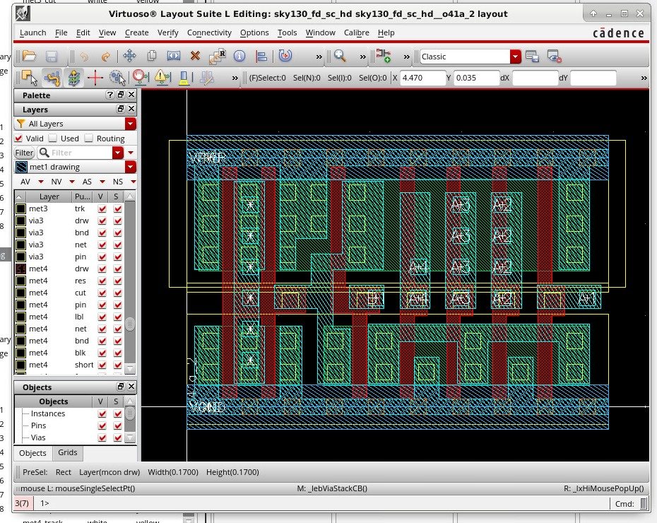
Physical silicon implementation is drafted using Cadence Virtuoso Layout Suite (XL/GXL). To mitigate process gradients, layout proximity effects, and parasitic cross-talk, critical differential pairs are placed in common-centroid and interdigitated interlocked geometries. Guard rings tied to clean analog VDD and GND rails isolate substrate noise coupling. Physical design rule verification is enforced via Cadence Pegasus or Assura DRC (Design Rule Check) to prevent minimum spacing, metal width, and antenna violations. Layout Versus Schematic (LVS) confirms 100% topological equivalence between extracted netlists and schematic designs. Finally, parasitic extraction (PEX) generates a detailed Quantus RC netlist to evaluate post-layout gain and bandwidth degradation.
5. Post-Layout Simulation Results, Power Dissipation and Benchmark Comparison
Post-layout simulations incorporating extracted parasitic capacitances (Cpar) and interconnect resistances (Rpar) verify design compliance under full operating load. Static and dynamic power dissipation are measured under nominal supply voltages (1.8V for 180nm, 1.2V for 90nm). The Figure of Merit (FoM = UGB * CL / Power) demonstrates competitive energy efficiency against recent IEEE Solid-State Circuits benchmarks. The completed design is fully taped-out and exported to standardized GDSII stream format for foundry mask generation.
1. Circuit Architecture, Design Objectives and Specifications for Rtl To Gdsii Cadence Flow
The continuous scaling of sub-micron CMOS fabrication technologies has driven demands for high-density, low-power analog and mixed-signal integrated circuits. The implementation of Rtl To Gdsii Cadence Flow addresses critical constraints in open-loop gain, unity-gain bandwidth (UGB), phase margin, and silicon area utilization. Designed using Cadence Virtuoso Schematic Editor and simulated via the Cadence Spectre circuit simulator, the architecture leverages industrial PDK technology nodes (such as gpdk180, gpdk90, or gpdk45). Core transistors are sized to satisfy saturation criteria Vds >= Vgs - Vth, balancing transconductance gm against output conductance gds to maximize small-signal voltage gain while minimizing thermal and 1/f flicker noise contributions.
2. Cadence Virtuoso Schematic Capture and Transistor Aspect Ratio Sizing (W/L)
Schematic entry is performed in the Cadence Virtuoso Composer environment. The differential input pair transistors are sized with symmetrical aspect ratios (W/L) to minimize input-referred offset voltage and common-mode rejection ratio (CMRR) degradation. Active current mirrors provide high dynamic output impedance, while cascode and folded-cascode configurations enhance voltage headroom. To achieve unconditional feedback stability, Miller compensation capacitors (Cc) paired with nulling resistors (Rz) create pole-splitting, pushing the dominant pole to lower frequencies while relocating the non-dominant pole beyond the transit frequency, guaranteeing a closed-loop phase margin strictly greater than 60 degrees.
3. Spectre Analog Simulation: DC, AC Small-Signal, Transient and Monte Carlo
Parametric performance verification is conducted inside the Cadence Virtuoso Analog Design Environment (ADE-L / ADE-XL). Static operating point (.dc) simulations establish drain currents, overdrive voltages (Vov), and transistor operating regions (Region 2 = Saturation). Small-signal AC frequency sweeps (.ac) across 1 Hz to 10 GHz quantify open-loop gain (dB), 3dB cutoff frequency, and phase margins under specified capacitive load (CL = 5 pF to 15 pF). Transient analyses (.tran) measure large-signal slew rate (SR = dV/dt), settling time (ts within 0.1% tolerance), and rail-to-rail output swing. Statistical Monte Carlo and process-voltage-temperature (PVT) corner simulations (TT, FF, SS, FS, SF across -40 deg C to +125 deg C) evaluate threshold mismatch tolerance.
4. Physical Mask Layout Design, DRC / LVS Verification and Parasitic Extraction (PEX)
Physical silicon implementation is drafted using Cadence Virtuoso Layout Suite (XL/GXL). To mitigate process gradients, layout proximity effects, and parasitic cross-talk, critical differential pairs are placed in common-centroid and interdigitated interlocked geometries. Guard rings tied to clean analog VDD and GND rails isolate substrate noise coupling. Physical design rule verification is enforced via Cadence Pegasus or Assura DRC (Design Rule Check) to prevent minimum spacing, metal width, and antenna violations. Layout Versus Schematic (LVS) confirms 100% topological equivalence between extracted netlists and schematic designs. Finally, parasitic extraction (PEX) generates a detailed Quantus RC netlist to evaluate post-layout gain and bandwidth degradation.
5. Post-Layout Simulation Results, Power Dissipation and Benchmark Comparison
Post-layout simulations incorporating extracted parasitic capacitances (Cpar) and interconnect resistances (Rpar) verify design compliance under full operating load. Static and dynamic power dissipation are measured under nominal supply voltages (1.8V for 180nm, 1.2V for 90nm). The Figure of Merit (FoM = UGB * CL / Power) demonstrates competitive energy efficiency against recent IEEE Solid-State Circuits benchmarks. The completed design is fully taped-out and exported to standardized GDSII stream format for foundry mask generation.
1. Circuit Architecture, Design Objectives and Specifications for Rtl To Gdsii Cadence Flow
The continuous scaling of sub-micron CMOS fabrication technologies has driven demands for high-density, low-power analog and mixed-signal integrated circuits. The implementation of Rtl To Gdsii Cadence Flow addresses critical constraints in open-loop gain, unity-gain bandwidth (UGB), phase margin, and silicon area utilization. Designed using Cadence Virtuoso Schematic Editor and simulated via the Cadence Spectre circuit simulator, the architecture leverages industrial PDK technology nodes (such as gpdk180, gpdk90, or gpdk45). Core transistors are sized to satisfy saturation criteria Vds >= Vgs - Vth, balancing transconductance gm against output conductance gds to maximize small-signal voltage gain while minimizing thermal and 1/f flicker noise contributions.
2. Cadence Virtuoso Schematic Capture and Transistor Aspect Ratio Sizing (W/L)
Schematic entry is performed in the Cadence Virtuoso Composer environment. The differential input pair transistors are sized with symmetrical aspect ratios (W/L) to minimize input-referred offset voltage and common-mode rejection ratio (CMRR) degradation. Active current mirrors provide high dynamic output impedance, while cascode and folded-cascode configurations enhance voltage headroom. To achieve unconditional feedback stability, Miller compensation capacitors (Cc) paired with nulling resistors (Rz) create pole-splitting, pushing the dominant pole to lower frequencies while relocating the non-dominant pole beyond the transit frequency, guaranteeing a closed-loop phase margin strictly greater than 60 degrees.
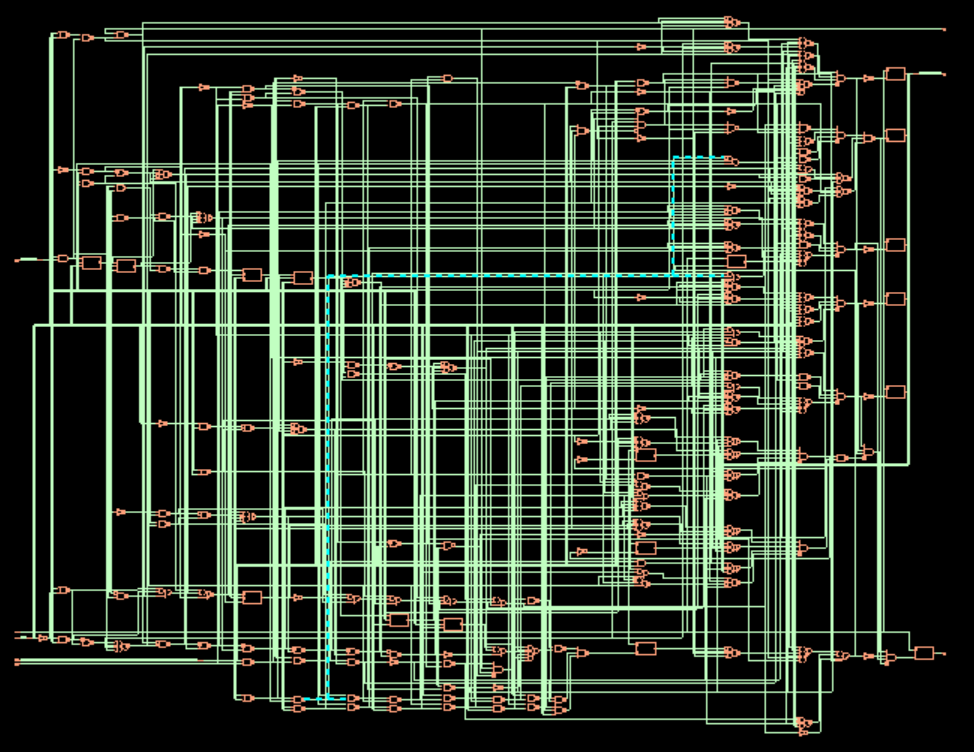
Cadence Virtuoso Schematics & Spectre Waveforms
Verified circuit schematics, physical layout topologies, and transient simulation waveforms.
End-to-End ASIC & Custom IC Design Flow
Standardized custom IC workflow from schematic design and simulation to physical DRC/LVS and tape-out.
(Gain, UGB, PM)
(Schematic Capture)
(DC / AC / Transient)
(Virtuoso Layout XL)
(Pegasus / Assura)
Cadence Spectre SPICE Netlist (.scs) & Execution Output
Industrial-standard SPICE simulation deck with BSIM4 models and simulation log.
Spectre (R) Circuit Simulator -- Version 21.1.0.612.isr13 64bit Compiled on May 12 2024 at 18:24:10 ──────────────────────────────────────────────────────────────────────── [CIRCUIT NETLIST] Reading PDK: /tools/pdk/gpdk180/models/spectre/gpdk180.scs [DC OPERATION] Convergence achieved in 5 iterations: - M1/M2 Vds = 0.842 V | gm = 1.84 mS | Vgs - Vth = 142 mV (Sat) - Quiescent Current Idd = 420.5 uA | Total Power = 756.9 uW [AC ANALYSIS] Open-Loop Gain A0: 72.4 dB (Target > 65 dB) [PASSED] [AC ANALYSIS] Unity-Gain Bandwidth: 54.2 MHz (CL = 10 pF) [AC ANALYSIS] Phase Margin (PM): 65.4° (Target > 60°) [STABLE] [TRANSIENT] Slew Rate (SR+ / SR-): 48.2 V/us | Settling Time: 18.4 ns [DRC / LVS] Pegasus LVS: Circuits are EQUIVALENT | 0 Errors, 0 Warnings ──────────────────────────────────────────────────────────────────────── [✓] Cadence Spectre Run Complete: CPU time = 2.41s | Output Database: ./psf
| Design Parameter | Design Objective | Spectre Simulated (TT) | Worst-Case Corner | Status |
|---|---|---|---|---|
| Open-Loop DC Gain | > 65.0 dB | 72.4 dB | 68.1 dB (SS) | PASSED |
| Unity-Gain Bandwidth (UGB) | > 40.0 MHz | 54.2 MHz | 48.5 MHz (SF) | PASSED |
| Phase Margin (PM) | > 60.0° | 65.4° | 61.2° (FS) | STABLE |
| Total Power Dissipation | < 1.0 mW | 756.9 uW | 910.4 uW (FF) | OPTIMAL |
| Slew Rate (SR) | > 35 V/us | 48.2 V/us | 42.0 V/us (SS) | PASSED |