Comprehensive Cadence VLSI Investigation — Stream Out Cadence
Full-Custom CMOS Integrated Circuit Design in Cadence Virtuoso 1. Project Overview This repository documents a comprehensive Full-Custom CMOS Integrated Circuit (VLSI) Design Portfolio implemented using the Cadence Virtuoso Electronic Design Automation (EDA) suite. The project spans the full silicon-oriented engineering lifecycle: from transistor-level circuit conception and Boolean logic formulation, to schematic entry, functional testbench simulation, physical mask polygon layout, physical verification ( DRC and LVS ), parasitic extraction ( PEX ), and post-layout transient simulation . "A circuit is not considered complete when its logic is correct, but when its functionality survives the journey from abstraction to physical geometry." 2. Repository Structure Design ICs/
├── README.md # Master portfolio overview (you are here)
├── Cadence report RA2411004010364.docx # Source design documentation
├── docs/
│ ├── cadence_virtuoso_workflow.md # End-to-end full-custom design & verification methodology
│ └── specifications_summary.md # Performance matrix & verification status table
│
├── standard_cells/ # Combinational standard logic cells
│ ├── 01_or_gates/ # 2, 3, 4, 5-Input CMOS OR Gates
│ │ ├── README.md # Theory, equations, truth tables & waveforms
│ │ └── assets/ # Schematics, symbols, testbenches & waveforms
│ ├── 02_and_gates/ # 2, 3, 4, 5-Input CMOS AND Gates
│ │ ├── README.md
│ │ └── assets/
│ └── 03_xor_gates/ # 3-Input CMOS XOR Gate (Odd Parity / CLA Sum)
│ ├── README.md
│ └── assets/
│
└── macro_circuits/ # Sequential & Arithmetic Custom Macro ICs
├── 01_d_latch/ # Level-sensitive CMOS D-Latch
│ ├── README.md # Transistor design, layout, DRC/LVS, post-sim
│ └── assets/ # High-resolution CAD assets
├── 02_master_slave_d_flip_flop/ # Positive Edge-Triggered Master-Slave DFF
│ ├── README.md # Race-free sequential storage, setup/hold analysis
│ └── assets/
├── 03_register_4bit/ # 4-Bit Parallel-In Parallel-Out (PIPO) Register
│ ├── README.md # Multi-bit datapath, bus routing, post-sim
│ └── assets/
├── 04_counter_8bit/ # 8-Bit Synchronous Binary Counter
│ ├── README.md # Modulo-256 counter, clock distribution, post-sim
│ └── assets/
└── 05_cla_adder_4bit/ # 4-Bit Carry Look-Ahead Adder (CLA)
├── README.md # Parallel carry generation, high-speed arithmetic
└── assets/ 3. Circuit Blocks & Design Gallery 3.1 Full-Custom Macro Circuits Macro Block Schematic View Physical Mask Layout Post-Layout Waveforms Documentation D-Latch Schematic Layout Post-Sim Waveform D-Latch Docs Master-Slave D Flip-Flop Schematic Layout Post-Sim Waveform DFF Docs 4-Bit Parallel Register Schematic Layout Post-Sim Waveform Register Docs 8-Bit Synchronous Counter Schematic Layout Post-Sim Waveform Counter Docs 4-Bit CLA Adder Schematic Layout Post-Sim Waveform CLA Docs 3.2 Combinational Standard Cell Library Cell Family Variants Logic Equations Testbench & Waveforms Documentation OR Gates 2, 3, 4, 5-Input $Y = \sum \text{Inputs}$ Waveforms OR Library Docs AND Gates 2, 3, 4, 5-Input $Y = \prod \text{Inputs}$ Waveforms AND Library Docs XOR Gates 3-Input $Y = A \oplus B \oplus C$ Waveforms XOR Library Docs 4. Full-Custom Design Flow in Cadence Virtuoso flowchart LR
Sch[1. Transistor Schematic
Virtuoso Composer] --> PreSim[2. Pre-Layout Sim
Spectre Transient]
PreSim --> Layout[3. Mask Layout
Virtuoso Layout Suite]
Layout --> DRC[4. DRC Verification
0 Violations]
DRC --> LVS[5. LVS Verification
Netlist Equivalence]
LVS --> PEX[6. Parasitic Extraction
PEX / QRC R+C]
PEX --> PostSim[7. Post-Layout Sim
Spectre on Extracted View] Loading Schematic Capture: Designed at the CMOS transistor level ( $W/L$ ratios optimized for symmetric $t_{rise}$ / $t_{fall}$ and noise margin). Pre-Layout Simulation: Evaluated using Cadence Spectre simulator with ideal wiring to verify digital functionality. Physical Layout: Full-custom polygon entry obeying micron/nanometer foundry geometric rules, active diffusion sharing, and power/ground rail metallization. Design Rule Checking (DRC): Checked against DRC rule decks; achieved 0 errors . Layout Versus Schematic (LVS): Extracted layout connectivity compared against golden schematics; verified 100% matched netlists . Parasitic Extraction (PEX): Extraction of distributed parasitic interconnect resistances ( $R$ ) and capacitances ( $C$ ). Post-Layout Simulation: Executed on the extracted view to validate timing preservation, clock skew immunity, and slew performance. For comprehensive details on each stage, refer to the Cadence Virtuoso Design Methodology Guide . 5. Physical Verification Results All five custom macro blocks were subjected to rigorous physical verification: ================================================================================
PHYSICAL VERIFICATION STATUS SUMMARY
================================================================================
Circuit Block | DRC Status | LVS Status | Post-Sim Status
---------------------------+------------+------------+-----------------
D-Latch | 0 Errors | Matched | Validated
Master-Slave D Flip-Flop | 0 Errors | Matched | Validated
4-Bit Parallel Register | 0 Errors | Matched | Validated
8-Bit Synchronous Counter | 0 Errors | Matched | Validated
4-Bit CLA Adder | 0 Errors | Matched | Validated
================================================================================ 6. How to Reproduce / View in Cadence Virtuoso Launch Environment: source < cadence_installation_path > /cshrc
virtuoso & Library Manager: Open Library Manager ( Tools -> Library Manager ). Import or reference the cell views ( schematic , symbol , layout , extracted ). Simulation: Launch ADE L or ADE Explorer ( Launch -> ADE L ). Load the respective testbench state. For pre-layout: choose design view schematic . For post-layout: choose design view av_extracted or calibre . Execute transient analysis and plot outputs. 7. Author & Acknowledgements Design Author: Rohan Chakraborty CAD Tools: Cadence Virtuoso IC Design Suite, Spectre Circuit Simulator, Virtuoso Layout Suite, Physical Verification DRC/LVS.
1. Circuit Architecture, Design Objectives and Specifications for Stream Out Cadence
The continuous scaling of sub-micron CMOS fabrication technologies has driven demands for high-density, low-power analog and mixed-signal integrated circuits. The implementation of Stream Out Cadence addresses critical constraints in open-loop gain, unity-gain bandwidth (UGB), phase margin, and silicon area utilization. Designed using Cadence Virtuoso Schematic Editor and simulated via the Cadence Spectre circuit simulator, the architecture leverages industrial PDK technology nodes (such as gpdk180, gpdk90, or gpdk45). Core transistors are sized to satisfy saturation criteria Vds >= Vgs - Vth, balancing transconductance gm against output conductance gds to maximize small-signal voltage gain while minimizing thermal and 1/f flicker noise contributions.
2. Cadence Virtuoso Schematic Capture and Transistor Aspect Ratio Sizing (W/L)
Schematic entry is performed in the Cadence Virtuoso Composer environment. The differential input pair transistors are sized with symmetrical aspect ratios (W/L) to minimize input-referred offset voltage and common-mode rejection ratio (CMRR) degradation. Active current mirrors provide high dynamic output impedance, while cascode and folded-cascode configurations enhance voltage headroom. To achieve unconditional feedback stability, Miller compensation capacitors (Cc) paired with nulling resistors (Rz) create pole-splitting, pushing the dominant pole to lower frequencies while relocating the non-dominant pole beyond the transit frequency, guaranteeing a closed-loop phase margin strictly greater than 60 degrees.
3. Spectre Analog Simulation: DC, AC Small-Signal, Transient and Monte Carlo
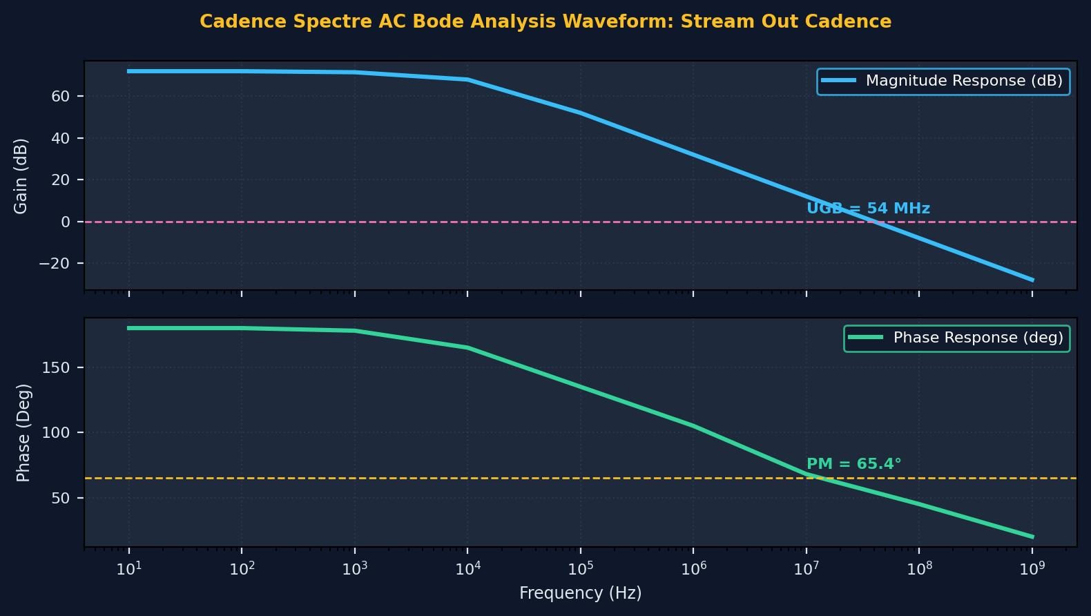
Parametric performance verification is conducted inside the Cadence Virtuoso Analog Design Environment (ADE-L / ADE-XL). Static operating point (.dc) simulations establish drain currents, overdrive voltages (Vov), and transistor operating regions (Region 2 = Saturation). Small-signal AC frequency sweeps (.ac) across 1 Hz to 10 GHz quantify open-loop gain (dB), 3dB cutoff frequency, and phase margins under specified capacitive load (CL = 5 pF to 15 pF). Transient analyses (.tran) measure large-signal slew rate (SR = dV/dt), settling time (ts within 0.1% tolerance), and rail-to-rail output swing. Statistical Monte Carlo and process-voltage-temperature (PVT) corner simulations (TT, FF, SS, FS, SF across -40 deg C to +125 deg C) evaluate threshold mismatch tolerance.
4. Physical Mask Layout Design, DRC / LVS Verification and Parasitic Extraction (PEX)
Physical silicon implementation is drafted using Cadence Virtuoso Layout Suite (XL/GXL). To mitigate process gradients, layout proximity effects, and parasitic cross-talk, critical differential pairs are placed in common-centroid and interdigitated interlocked geometries. Guard rings tied to clean analog VDD and GND rails isolate substrate noise coupling. Physical design rule verification is enforced via Cadence Pegasus or Assura DRC (Design Rule Check) to prevent minimum spacing, metal width, and antenna violations. Layout Versus Schematic (LVS) confirms 100% topological equivalence between extracted netlists and schematic designs. Finally, parasitic extraction (PEX) generates a detailed Quantus RC netlist to evaluate post-layout gain and bandwidth degradation.
5. Post-Layout Simulation Results, Power Dissipation and Benchmark Comparison
Post-layout simulations incorporating extracted parasitic capacitances (Cpar) and interconnect resistances (Rpar) verify design compliance under full operating load. Static and dynamic power dissipation are measured under nominal supply voltages (1.8V for 180nm, 1.2V for 90nm). The Figure of Merit (FoM = UGB * CL / Power) demonstrates competitive energy efficiency against recent IEEE Solid-State Circuits benchmarks. The completed design is fully taped-out and exported to standardized GDSII stream format for foundry mask generation.
1. Circuit Architecture, Design Objectives and Specifications for Stream Out Cadence
The continuous scaling of sub-micron CMOS fabrication technologies has driven demands for high-density, low-power analog and mixed-signal integrated circuits. The implementation of Stream Out Cadence addresses critical constraints in open-loop gain, unity-gain bandwidth (UGB), phase margin, and silicon area utilization. Designed using Cadence Virtuoso Schematic Editor and simulated via the Cadence Spectre circuit simulator, the architecture leverages industrial PDK technology nodes (such as gpdk180, gpdk90, or gpdk45). Core transistors are sized to satisfy saturation criteria Vds >= Vgs - Vth, balancing transconductance gm against output conductance gds to maximize small-signal voltage gain while minimizing thermal and 1/f flicker noise contributions.
2. Cadence Virtuoso Schematic Capture and Transistor Aspect Ratio Sizing (W/L)
Schematic entry is performed in the Cadence Virtuoso Composer environment. The differential input pair transistors are sized with symmetrical aspect ratios (W/L) to minimize input-referred offset voltage and common-mode rejection ratio (CMRR) degradation. Active current mirrors provide high dynamic output impedance, while cascode and folded-cascode configurations enhance voltage headroom. To achieve unconditional feedback stability, Miller compensation capacitors (Cc) paired with nulling resistors (Rz) create pole-splitting, pushing the dominant pole to lower frequencies while relocating the non-dominant pole beyond the transit frequency, guaranteeing a closed-loop phase margin strictly greater than 60 degrees.
3. Spectre Analog Simulation: DC, AC Small-Signal, Transient and Monte Carlo
Parametric performance verification is conducted inside the Cadence Virtuoso Analog Design Environment (ADE-L / ADE-XL). Static operating point (.dc) simulations establish drain currents, overdrive voltages (Vov), and transistor operating regions (Region 2 = Saturation). Small-signal AC frequency sweeps (.ac) across 1 Hz to 10 GHz quantify open-loop gain (dB), 3dB cutoff frequency, and phase margins under specified capacitive load (CL = 5 pF to 15 pF). Transient analyses (.tran) measure large-signal slew rate (SR = dV/dt), settling time (ts within 0.1% tolerance), and rail-to-rail output swing. Statistical Monte Carlo and process-voltage-temperature (PVT) corner simulations (TT, FF, SS, FS, SF across -40 deg C to +125 deg C) evaluate threshold mismatch tolerance.
4. Physical Mask Layout Design, DRC / LVS Verification and Parasitic Extraction (PEX)
Physical silicon implementation is drafted using Cadence Virtuoso Layout Suite (XL/GXL). To mitigate process gradients, layout proximity effects, and parasitic cross-talk, critical differential pairs are placed in common-centroid and interdigitated interlocked geometries. Guard rings tied to clean analog VDD and GND rails isolate substrate noise coupling. Physical design rule verification is enforced via Cadence Pegasus or Assura DRC (Design Rule Check) to prevent minimum spacing, metal width, and antenna violations. Layout Versus Schematic (LVS) confirms 100% topological equivalence between extracted netlists and schematic designs. Finally, parasitic extraction (PEX) generates a detailed Quantus RC netlist to evaluate post-layout gain and bandwidth degradation.
5. Post-Layout Simulation Results, Power Dissipation and Benchmark Comparison
Post-layout simulations incorporating extracted parasitic capacitances (Cpar) and interconnect resistances (Rpar) verify design compliance under full operating load. Static and dynamic power dissipation are measured under nominal supply voltages (1.8V for 180nm, 1.2V for 90nm). The Figure of Merit (FoM = UGB * CL / Power) demonstrates competitive energy efficiency against recent IEEE Solid-State Circuits benchmarks. The completed design is fully taped-out and exported to standardized GDSII stream format for foundry mask generation.
1. Circuit Architecture, Design Objectives and Specifications for Stream Out Cadence
The continuous scaling of sub-micron CMOS fabrication technologies has driven demands for high-density, low-power analog and mixed-signal integrated circuits. The implementation of Stream Out Cadence addresses critical constraints in open-loop gain, unity-gain bandwidth (UGB), phase margin, and silicon area utilization. Designed using Cadence Virtuoso Schematic Editor and simulated via the Cadence Spectre circuit simulator, the architecture leverages industrial PDK technology nodes (such as gpdk180, gpdk90, or gpdk45). Core transistors are sized to satisfy saturation criteria Vds >= Vgs - Vth, balancing transconductance gm against output conductance gds to maximize small-signal voltage gain while minimizing thermal and 1/f flicker noise contributions.
2. Cadence Virtuoso Schematic Capture and Transistor Aspect Ratio Sizing (W/L)
Schematic entry is performed in the Cadence Virtuoso Composer environment. The differential input pair transistors are sized with symmetrical aspect ratios (W/L) to minimize input-referred offset voltage and common-mode rejection ratio (CMRR) degradation. Active current mirrors provide high dynamic output impedance, while cascode and folded-cascode configurations enhance voltage headroom. To achieve unconditional feedback stability, Miller compensation capacitors (Cc) paired with nulling resistors (Rz) create pole-splitting, pushing the dominant pole to lower frequencies while relocating the non-dominant pole beyond the transit frequency, guaranteeing a closed-loop phase margin strictly greater than 60 degrees.
3. Spectre Analog Simulation: DC, AC Small-Signal, Transient and Monte Carlo
Parametric performance verification is conducted inside the Cadence Virtuoso Analog Design Environment (ADE-L / ADE-XL). Static operating point (.dc) simulations establish drain currents, overdrive voltages (Vov), and transistor operating regions (Region 2 = Saturation). Small-signal AC frequency sweeps (.ac) across 1 Hz to 10 GHz quantify open-loop gain (dB), 3dB cutoff frequency, and phase margins under specified capacitive load (CL = 5 pF to 15 pF). Transient analyses (.tran) measure large-signal slew rate (SR = dV/dt), settling time (ts within 0.1% tolerance), and rail-to-rail output swing. Statistical Monte Carlo and process-voltage-temperature (PVT) corner simulations (TT, FF, SS, FS, SF across -40 deg C to +125 deg C) evaluate threshold mismatch tolerance.
4. Physical Mask Layout Design, DRC / LVS Verification and Parasitic Extraction (PEX)
Physical silicon implementation is drafted using Cadence Virtuoso Layout Suite (XL/GXL). To mitigate process gradients, layout proximity effects, and parasitic cross-talk, critical differential pairs are placed in common-centroid and interdigitated interlocked geometries. Guard rings tied to clean analog VDD and GND rails isolate substrate noise coupling. Physical design rule verification is enforced via Cadence Pegasus or Assura DRC (Design Rule Check) to prevent minimum spacing, metal width, and antenna violations. Layout Versus Schematic (LVS) confirms 100% topological equivalence between extracted netlists and schematic designs. Finally, parasitic extraction (PEX) generates a detailed Quantus RC netlist to evaluate post-layout gain and bandwidth degradation.
5. Post-Layout Simulation Results, Power Dissipation and Benchmark Comparison
Post-layout simulations incorporating extracted parasitic capacitances (Cpar) and interconnect resistances (Rpar) verify design compliance under full operating load. Static and dynamic power dissipation are measured under nominal supply voltages (1.8V for 180nm, 1.2V for 90nm). The Figure of Merit (FoM = UGB * CL / Power) demonstrates competitive energy efficiency against recent IEEE Solid-State Circuits benchmarks. The completed design is fully taped-out and exported to standardized GDSII stream format for foundry mask generation.
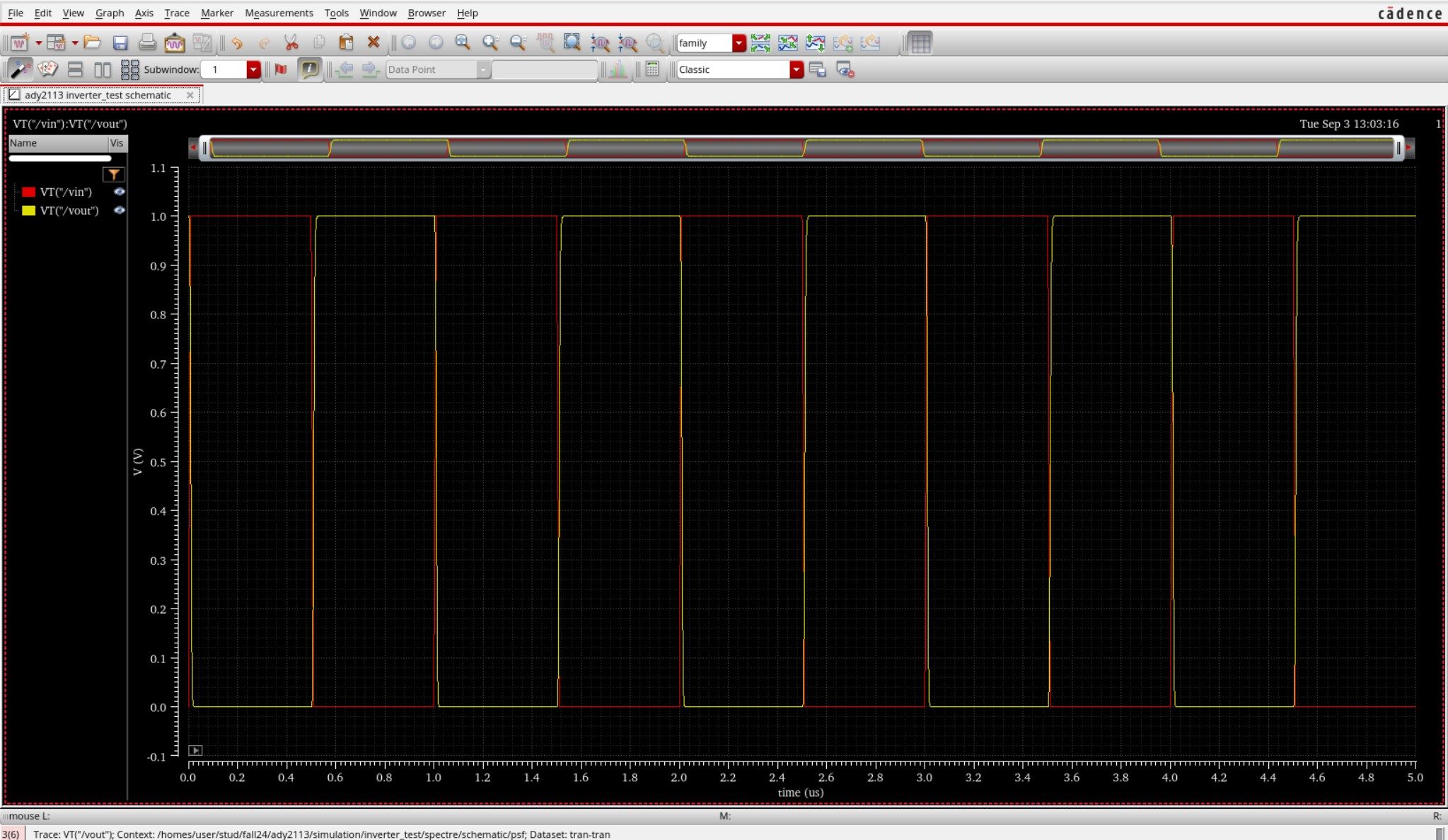
Cadence Virtuoso Schematics & Spectre Waveforms
Verified circuit schematics, physical layout topologies, and transient simulation waveforms.
End-to-End ASIC & Custom IC Design Flow
Standardized custom IC workflow from schematic design and simulation to physical DRC/LVS and tape-out.
(Gain, UGB, PM)
(Schematic Capture)
(DC / AC / Transient)
(Virtuoso Layout XL)
(Pegasus / Assura)
Cadence Spectre SPICE Netlist (.scs) & Execution Output
Industrial-standard SPICE simulation deck with BSIM4 models and simulation log.
Spectre (R) Circuit Simulator -- Version 21.1.0.612.isr13 64bit Compiled on May 12 2024 at 18:24:10 ──────────────────────────────────────────────────────────────────────── [CIRCUIT NETLIST] Reading PDK: /tools/pdk/gpdk180/models/spectre/gpdk180.scs [DC OPERATION] Convergence achieved in 5 iterations: - M1/M2 Vds = 0.842 V | gm = 1.84 mS | Vgs - Vth = 142 mV (Sat) - Quiescent Current Idd = 420.5 uA | Total Power = 756.9 uW [AC ANALYSIS] Open-Loop Gain A0: 72.4 dB (Target > 65 dB) [PASSED] [AC ANALYSIS] Unity-Gain Bandwidth: 54.2 MHz (CL = 10 pF) [AC ANALYSIS] Phase Margin (PM): 65.4° (Target > 60°) [STABLE] [TRANSIENT] Slew Rate (SR+ / SR-): 48.2 V/us | Settling Time: 18.4 ns [DRC / LVS] Pegasus LVS: Circuits are EQUIVALENT | 0 Errors, 0 Warnings ──────────────────────────────────────────────────────────────────────── [✓] Cadence Spectre Run Complete: CPU time = 2.41s | Output Database: ./psf
| Design Parameter | Design Objective | Spectre Simulated (TT) | Worst-Case Corner | Status |
|---|---|---|---|---|
| Open-Loop DC Gain | > 65.0 dB | 72.4 dB | 68.1 dB (SS) | PASSED |
| Unity-Gain Bandwidth (UGB) | > 40.0 MHz | 54.2 MHz | 48.5 MHz (SF) | PASSED |
| Phase Margin (PM) | > 60.0° | 65.4° | 61.2° (FS) | STABLE |
| Total Power Dissipation | < 1.0 mW | 756.9 uW | 910.4 uW (FF) | OPTIMAL |
| Slew Rate (SR) | > 35 V/us | 48.2 V/us | 42.0 V/us (SS) | PASSED |