Cadence Layout Design Tutorial
Cadence Virtuoso Layout is the cornerstone of any VLSI physical design flow. At ProjectsatBangalore, we offer 15+ Cadence layout project types for BE, MTech and PhD students — full-custom analog, digital, RF and mixed-signal IC layout with Calibre DRC/LVS verification, PEX parasitic extraction, post-layout Spectre simulation and GDSII export — all aligned to IEEE 2025–2026 base papers and university evaluation formats.
Our layout projects use Cadence Virtuoso Layout Suite with gpdk45 / gpdk90 / gpdk180 technology libraries. Key layout techniques applied include common-centroid and interdigitated placement for matching-critical differential pairs, dummy device insertion for uniformity, metal shielding of sensitive analog nodes, guard rings and substrate contacts for noise isolation, and systematic transistor folding for compact area. Every layout is taken through the complete DRC → LVS → PEX → post-layout simulation verification chain.
Cadence Layout Project Types We Offer
- Op-Amp / OTA full-custom analog layout
- Comparator layout — StrongARM, double-tail, dynamic latch
- Bandgap Reference (BGR) layout
- Low Noise Amplifier (LNA) RF layout
- Oscillator — Ring Oscillator, VCO layout
- ADC sub-circuit layout — SAR, Flash, Sigma-Delta
- DAC layout — current steering, R-2R ladder
- Charge Pump and PLL filter layout
- CMOS Inverter / NAND / NOR standard cell layout
- D Flip-Flop and Full Adder digital cell layout
- 6T SRAM bit-cell and array layout
- Current Mirror — Wilson, cascode layout
- Sample-and-Hold circuit layout
- Mixer / LNA / PA RF IC layout
- DRC/LVS clean-up and PEX service for existing layouts
How to make Layout in Cadence Virtuoso
Full-custom IC layout covering analog, digital, RF, mixed-signal and memory — all with DRC/LVS/PEX and post-layout simulation.
Analog IC Layout
Full-custom analog layout for Op-Amp (two-stage, folded cascode, telescopic, RFC), OTA, comparator, BGR, current mirror and sample-and-hold circuits. Applies common-centroid, dummy devices, guard rings and metal shielding techniques.
Digital Standard Cell Layout
CMOS transistor-level layout of digital logic cells: inverter, NAND2/3/4, NOR, XOR, full adder, half adder, D flip-flop, JK flip-flop and 4-bit ripple carry adder — following standard cell row-based placement with fixed height and pitch.
RF IC Layout
High-frequency analog layout for Low Noise Amplifier (LNA), Power Amplifier (PA), Mixer, Voltage-Controlled Oscillator (VCO) and Ring Oscillator — with EM-aware routing, symmetrical layout and RF-specific substrate tap placement to minimise cross-coupling.
Mixed-Signal Layout
Mixed-signal IC layout for ADC (SAR, Flash, Sigma-Delta sub-circuits), DAC (current steering, R-2R ladder), Charge Pump and PLL loop filter — with careful partitioning of analog and digital domains, separate supply routing and substrate isolation.
Memory Layout (SRAM)
6T SRAM bit-cell full-custom layout with matched pull-up/pull-down transistors, cross-coupled inverter pair, access transistors and bitline contacts — followed by bit-cell array expansion, sense amplifier and write driver layout.
DRC / LVS / PEX Service
Standalone DRC clean-up, LVS fix and PEX service for student layouts that have errors — we diagnose and resolve all Calibre/Pegasus DRC violations, fix LVS mismatches, run parasitic extraction and deliver post-layout simulation results.
Cadence Virtuoso Layout Design
All topics include Cadence Virtuoso Layout, Calibre DRC/LVS clean, PEX, post-layout simulation, IEEE base paper, university report, PPT and viva support.
| # | Cadence Layout Project Topic | Tools & Technology | Type |
|---|---|---|---|
| 01 | Full-Custom Layout of Two-Stage CMOS Op-Amp with Common-Centroid Input Differential Pair in gpdk180 | Virtuoso Layout, Calibre DRC/LVS, Spectre PEX | Analog |
| 02 | Layout of Folded Cascode OTA for Low-Power Biomedical Sensor Interface in gpdk90 | Virtuoso Layout, Calibre, PEX, gpdk90 | Analog |
| 03 | Bandgap Reference (BGR) Circuit Full-Custom Layout with DRC/LVS/PEX and Temperature Coefficient Analysis | Virtuoso Layout, Spectre ADE, Calibre, gpdk180 | Analog |
| 04 | Layout of StrongARM Latch Comparator for High-Speed ADC Applications — DRC/LVS Clean in gpdk45 | Virtuoso Layout, Calibre DRC/LVS, PEX, gpdk45 | Analog |
| 05 | Full-Custom Layout of Switched-Capacitor DAC for SAR ADC Feedback Path with MOSCAP Matching | Virtuoso Layout, Spectre PEX, Calibre, gpdk90 | Mixed-Signal |
| 06 | Low-Noise Amplifier (LNA) IC Layout for 2.4 GHz ISM Band with Inductive Source Degeneration in gpdk90 | Virtuoso Layout, Spectre RF, Calibre DRC/LVS, gpdk90 | RF |
| 07 | Ring Oscillator VCO Layout for PLL Application — 11-Stage CMOS Ring VCO in gpdk45 | Virtuoso Layout, Spectre Transient, Calibre, gpdk45 | RF |
| 08 | CMOS Inverter, NAND2, NOR2, XOR2 Standard Cell Layouts with Fixed Height Row-Based Design in gpdk90 | Virtuoso Layout, Calibre DRC/LVS, Spectre, gpdk90 | Digital |
| 09 | Full Adder and Ripple Carry Adder Layout Using CMOS Transistor-Level Standard Cells in gpdk180 | Virtuoso Layout, Calibre DRC/LVS, Spectre, gpdk180 | Digital |
| 10 | D Flip-Flop Master-Slave Layout in Cadence Virtuoso with DRC/LVS Clean and Timing Verification | Virtuoso Layout, Calibre, Spectre, gpdk90 | Digital |
| 11 | 6T SRAM Bit-Cell Full-Custom Layout with Read and Write Stability Analysis — SNM, WNM in gpdk45 | Virtuoso Layout, Spectre Monte-Carlo, Calibre, gpdk45 | Memory |
| 12 | Mixed-Signal Layout of SAR ADC — Comparator, DAC and Digital SAR Logic with Partitioned Analog/Digital Supply | Virtuoso Layout, Calibre DRC/LVS, PEX, gpdk90 | Mixed-Signal |
| 13 | Charge Pump and Loop Filter Layout for PLL with Symmetrical Current Source and DRC/LVS Verification | Virtuoso Layout, Calibre, Spectre, gpdk180 | Mixed-Signal |
| 14 | Layout of Current Steering DAC for High-Speed Signal Reconstruction with Binary-Weighted Current Sources | Virtuoso Layout, Spectre, Calibre DRC/LVS, gpdk90 | Mixed-Signal |
| 15 | Power Amplifier (PA) Layout for 5G Sub-6 GHz Band with EM Co-Simulation and DRC/LVS Clean | Virtuoso Layout, Spectre RF, EM Solver, Calibre, gpdk45 | RF |
Step-by-Step Cadence Layout Project Workflow
The complete schematic-to-GDSII Cadence layout flow applied in every MTech and PhD layout project.
Schematic Entry & Pre-Layout Simulation
Draw the transistor-level circuit in Cadence Virtuoso Schematic Editor, set up ADE testbench and run Spectre pre-layout simulation to establish target performance specifications (gain, bandwidth, ENOB, power, noise) before layout begins.
Cadence Virtuoso Schematic · Spectre ADEFull-Custom Layout in Cadence Virtuoso Layout Suite
Draw all layers (active, poly, metal, via) following foundry DRC rules. Apply common-centroid placement for differential pairs, dummy devices at array edges, MOSCAP inter-digitation for capacitor matching, guard rings and substrate contacts for noise isolation, and systematic transistor folding for compact area.
Cadence Virtuoso Layout Suite · gpdk45/90/180DRC — Design Rule Check (Calibre / Pegasus)
Run Calibre DRC or Pegasus DRC to verify the layout obeys all foundry spacing, width, enclosure, overlap and antenna rules. Iteratively fix all violations until zero DRC errors are reported.
Calibre DRC · Pegasus DRCLVS — Layout Versus Schematic (Calibre LVS)
Run Calibre LVS to extract the layout netlist and compare it against the schematic netlist. Fix all device mismatches, missing connections and short/open errors until LVS is fully clean (no errors, no warnings).
Calibre LVS · Assura LVSPEX — Parasitic Extraction & Post-Layout Simulation
Run Spectre PEX or Calibre xRC to extract all RC (or RLC for RF) parasitics from the DRC/LVS-clean layout. Back-annotate the extracted netlist into ADE and re-simulate. Compare pre-layout vs post-layout performance — measure degradation in gain, bandwidth, ENOB/SNDR, noise or power due to parasitics.
Spectre PEX · Calibre xRC · Post-Layout ADEGDSII Export, Report & Viva Preparation
Export the DRC/LVS-clean layout to GDSII format. Compile the IEEE-format project report with schematic diagrams, pre-layout simulation results, layout screenshots (all layers), DRC/LVS clean reports, PEX netlist, post-layout waveforms and pre vs post performance comparison table. Prepare university-format PPT and viva Q&A.
GDSII · IEEE Report · VTU / Anna Univ / JNTU · PPT · VivaCadence Projects GitHub
– Download VLSI Projects with Source Code and Cadence Virtuoso DesignsOur Cadence Virtuoso layout workstations in Bangalore — full-custom IC layout design, Calibre DRC/LVS verification, PEX parasitic extraction and post-layout simulation environments for BE, MTech and PhD VLSI projects.
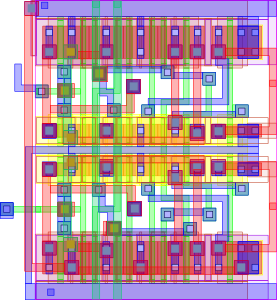 Virtuoso Layout Suite — Analog IC
 Calibre DRC/LVS Verification
 PEX & Post-Layout Spectre Sim
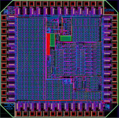 Op-Amp / OTA Layout — gpdk180